


Mechanism of voltage spike production during switching transients and its suppression methods in Boost converter
-
摘要:
Boost变换器常用作两级式逆变器的前级升压电路,由于电路中寄生参数的存在,开关瞬间输出电压叠加有瞬态尖峰,降低了波形质量,甚至影响逆变器的正常工作。为了抑制直流环节电压尖峰,研究了Boost电路开关瞬态过程,针对瞬态电路开关特性和开关器件工作状态,建立了基于金属氧化物半导体场效应晶体管(MOSFET)和肖特基二极管(SBD)的换流单元的解析模型,进一步分析了不同寄生参数对开关瞬态电流特性的影响,以及导致电压尖峰的机理等。仿真分析了寄生参数与输出电压尖峰大小的关系,提出了“减缓开关速度”和“降低输出端寄生电感”2种从源头抑制输出电压尖峰的方法。仿真和实验表明,这2种抑制方法能够有效减小电压尖峰,提高Boost电路的输出电压性能。
Abstract:Boost converter is often used as the pre-stage circuit in double-stage inverter. Because of the existence of parasitic parameters in the circuit, the output voltage will be superimposed with transient spikes, which reduces the waveform quality and even affects the operation of inverter. In order to suppress the voltage spikes, the switching transient of Boost converter is studied. Aimed at the switching characteristics of transient circuit and the operation status of switching devices, an analytical model of commutation unit based on metal-oxide-semiconductor field-effect transistor (MOSFET) and Schottky barrier diode (SBD) is established, and the influence of parasitic parameters on the current characteristics during switching transient, as well as the mechanism of causing voltage spikes, is analyzed. The relationships between the parasitic parameters and the output voltage spikes are analyzed and compared by simulation, and two methods are proposed to suppress the output voltage spikes, which are "slowing down the switching speed" and "reducing the output terminal parasitic inductance". The validity of these two methods to reduce voltage spikes and improve output voltage performance of Boost converters has been verified by simulation and experiments.
-
Key words:
- Boost converter /
- switching characteristics /
- voltage spikes /
- transient model /
- parasitic parameters
-

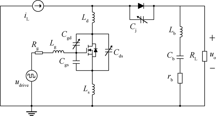
图 1 考虑寄生参数的Boost变换器等效电路
Figure 1. Equivalent circuit of Boost converter with parasitic parameters

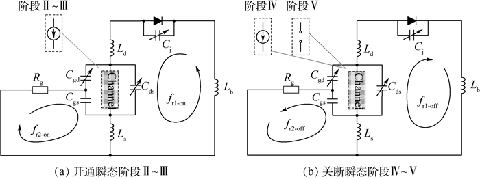
图 5 Boost变换器在开通瞬态阶段Ⅱ~Ⅲ和关断瞬态阶段Ⅳ~Ⅴ等效电路
Figure 5. Equivalent circuits of Boost converter in transient phase Ⅱ-Ⅲ of turn-on and phase Ⅳ-Ⅴ of turn-off

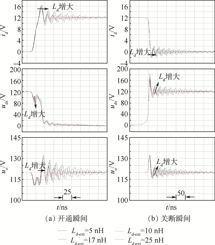
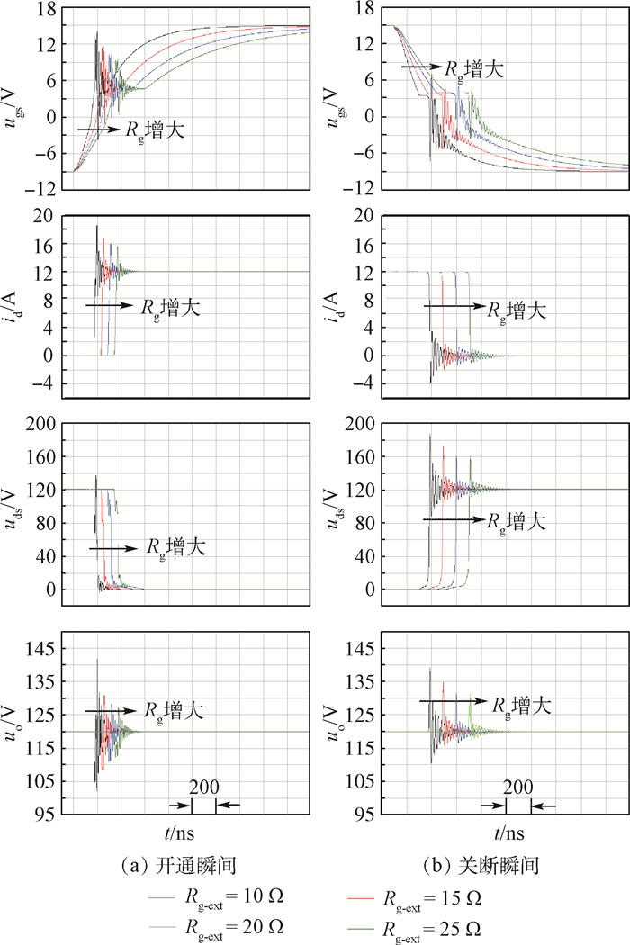
图 9 不同寄生电感及驱动电阻下的开关瞬间电压过冲
Figure 9. Switching transient voltage overshoots with different parasitic inductance and driving resistance

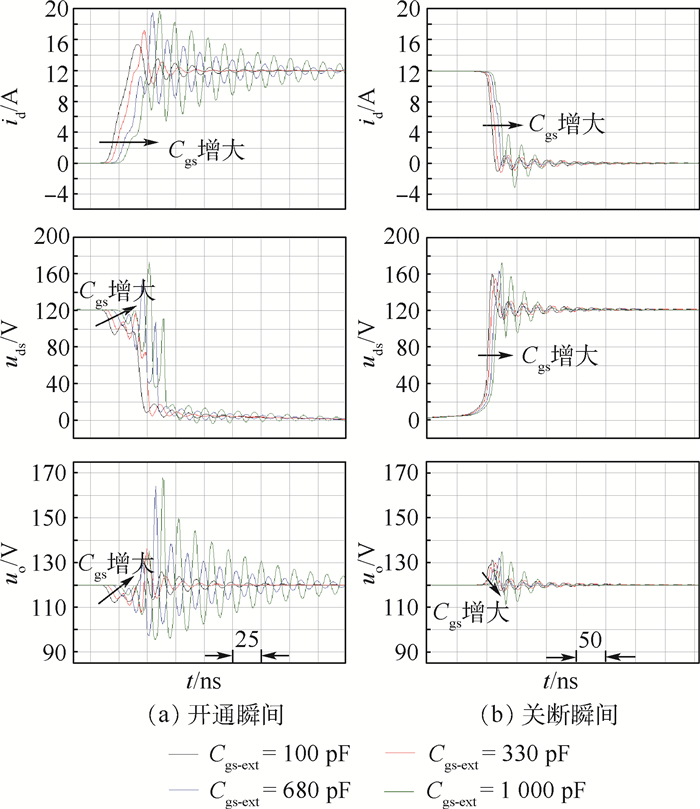
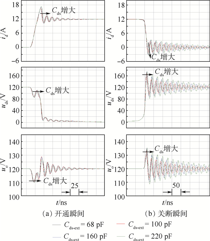
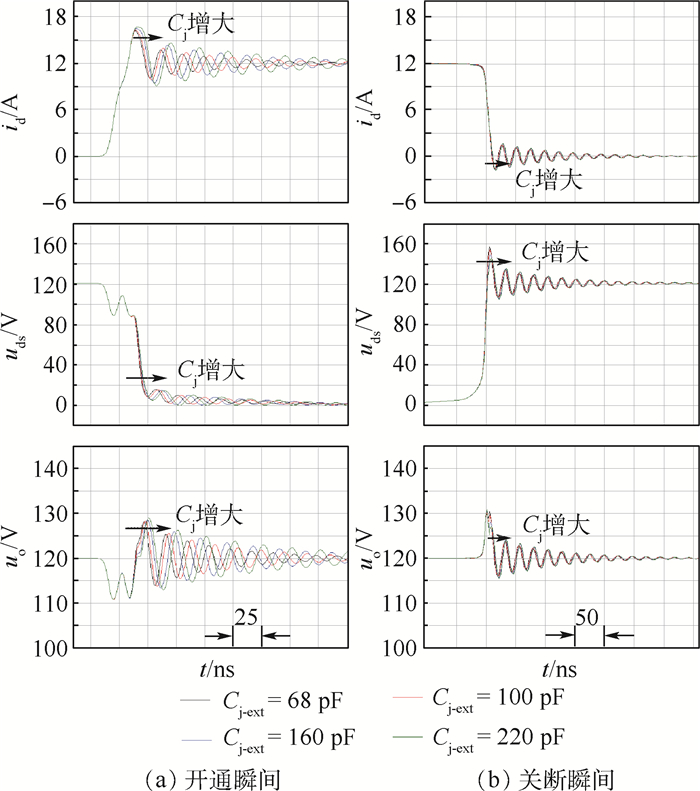
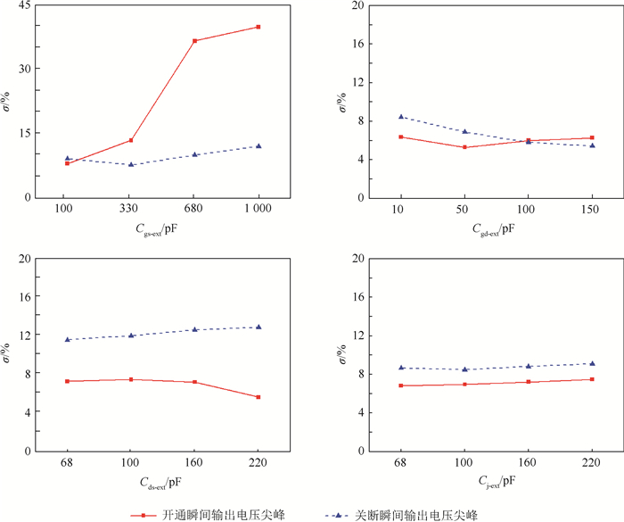
图 14 不同寄生电容下的开关瞬间电压过冲
Figure 14. Switching transient voltage overshoots with different parasitic capacitance

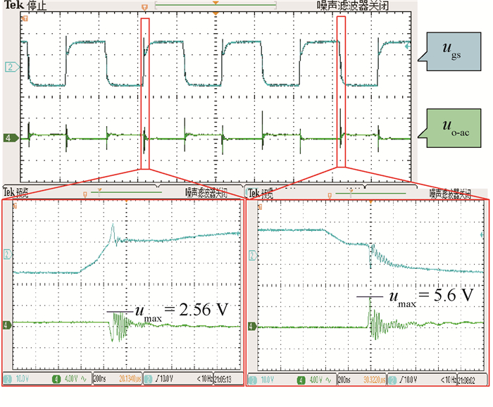
图 16 优化前开关瞬间输出电压交流分量波形
Figure 16. Ac-component waveform of output voltage of switching transient before optimization

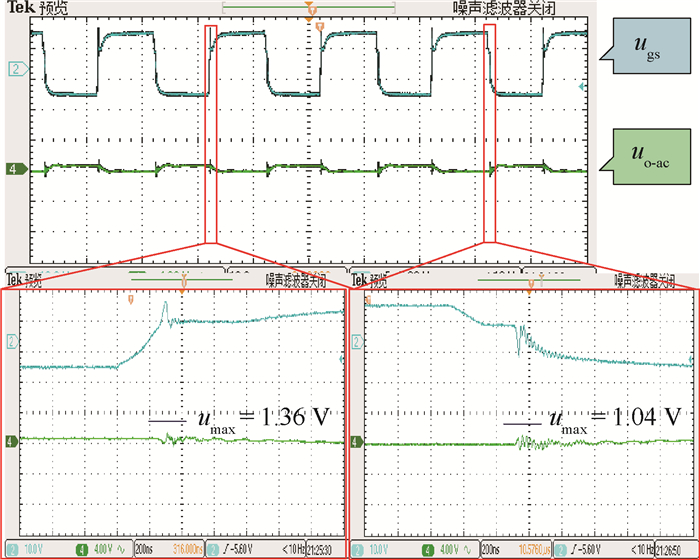
图 17 减缓开关速度后开关瞬间输出电压交流分量波形
Figure 17. Ac-component waveform of output voltage of switching transient after slowing down switching speed

图 18 减小输出端寄生电感后开关瞬间输出电压交流分量波形
Figure 18. Ac-component waveform of output voltage of switching transient after reducing parasitic inductance of output end

图 19 不同驱动电阻下MOSFET在开关瞬间的能量耗散图和Boost变换器的效率曲线
Figure 19. Energy dissipation diagram of MOSFET at switching moment and efficiency curve of Boost converter with different driving resistors
表 1 测试电路参数
Table 1. Parameters of test circuit
模块 参数 数值 功率回路 uo-dc/V 120 L/μH 420 Cbuffer/μF 680 RL/Ω 20 驱动回路 UCC/V 15 UEE/V -9 D/% 50 fs/kHz 50  下载: 导出CSV
-
[1] WANG J, JI B, LU X, et al.Steady-state and dynamic input current low-frequency ripple evaluation and reduction in two-stage single-phase inverters with back current gain model[J].IEEE Transactions on Power Electronics, 2014, 29(8):4247-4260. doi: 10.1109/TPEL.2013.2292609 [2] 杜青, 崔波, 夏宁, 等.一种新型大功率升降压变换器及控制方法[J].北京航空航天大学学报, 2017, 43(3):472-480. doi: 10.13700/j.bh.1001-5965.2016.0225DU Q, CUI B, XIA N, et al.A novel high-power step-up/step-down converter and control methods[J].Journal of Beijing University of Aeronautics and Astronautics, 2017, 43(3):472-480(in Chinese). doi: 10.13700/j.bh.1001-5965.2016.0225 [3] 张厚升, 赵艳雷.单相双级式光伏并网逆变器[J].电力自动化设备, 2010, 30(8):95-99. doi: 10.3969/j.issn.1006-6047.2010.08.020ZHANG H S, ZHAO Y L.Single-phase double-stage photovoltaic grid-connected inverter[J].Electric Power Automation Equipment, 2010, 30(8):95-99(in Chinese). doi: 10.3969/j.issn.1006-6047.2010.08.020 [4] TIAN Y, YANG X, XIE R, et al.A passive component based gate drive scheme for negative gate voltage spike mitigation in a sic-based dual-active bridge[C]//2018 IEEE Energy Conversion Congress and Exposition (ECCE).Piscataway, NJ: IEEE Press, 2018: 1841-1845. [5] WU Q, WANG Q, XIAO L, et al.One adaptive turn-off method for PFC converter with voltage spike limitation[C]//2016 IEEE Applied Power Electronics Conference and Exposition (APEC).Piscataway, NJ: IEEE Press, 2016: 1657-1662. https://www.researchgate.net/publication/303513910_One_adaptive_turn-off_method_for_PFC_converter_with_voltage_spike_limitation [6] PATEL H K.Voltage transient spikes suppression in flyback converter using dissipative voltage snubbers[C]//2008 3rd IEEE Conference on Industrial Electronics and Applications. Piscataway, NJ: IEEE Press, 2008: 897-901. 224321871_Voltage_transient_spikes_suppression_in_flyback_converter_using_dissipative_voltage_snubbers [7] WANG J, CHUNG S H, LI T H.Characterization and experimental assessment of the effects of parasitic elements on the MOSFET switching performance[J].IEEE Transactions on Power Electronics, 2012, 28(1):573-590. http://www.wanfangdata.com.cn/details/detail.do?_type=perio&id=05e0f54b81a849afa495060dad80a100 [8] CASTRO I, ROIG J, GELAGAEV R, et al. Analytical switching loss model for superjunction MOSFET with capacitive nonlinearities and displacement currents for DC-DC power converters[J].IEEE Transactions on Power Electronics, 2016, 31(3):2485-2495. doi: 10.1109/TPEL.2015.2433017 [9] CHEN Z, BOROYEVICH D, BURGOS R.Experimental parametric study of the parasitic inductance influence on MOSFET switching characteristics[C]//2010 International Power Electronics Conference(ECCE).Piscataway, NJ: IEEE Press, 2010: 164-169. 224165533_Experimental_parametric_study_of_the_parasitic_inductance_influence_on_MOSFET_switching_characteristics [10] 朱义诚, 赵争鸣, 王旭东, 等.SiC MOSFET与SiC SBD换流单元瞬态模型[J].电工技术学报, 2017, 32(12):58-69. http://www.wanfangdata.com.cn/details/detail.do?_type=perio&id=dgjsxb201712009ZHU Y C, ZHAO Z M, WANG X D, et al.Analytical transient model of commutation units with SiC MOSFET and SiC SBD pair[J].Transactions of China Electrotechnical Society, 2017, 32(12):58-69(in Chinese). http://www.wanfangdata.com.cn/details/detail.do?_type=perio&id=dgjsxb201712009 [11] CUI T, MA Q, XU P, et al.Analysis and optimization of power MOSFETs shaped switching transients for reduced EMI generation[J].IEEE Access, 2017, 5(1):20440-20448. http://cn.bing.com/academic/profile?id=7713a0c8808a24b764d8aa817fedc4ef&encoded=0&v=paper_preview&mkt=zh-cn [12] ENGELMANN G, SENONER T, DONCKER R W D.Experimental investigation on the transient switching behavior of SiC MOSFETs using a stage-wise gate driver[J].CPSS Transactions on Power Electronics and Applications, 2018, 3(1):77-87. doi: 10.24295/CPSSTPEA.2018.00008 [13] 罗剑波, 范伟, 彭凯.SiC MOSFET模块高频吸收电路研究[J].大功率变流技术, 2016, 5(1):23-30. http://www.wanfangdata.com.cn/details/detail.do?_type=perio&id=dglbljs201605006LUO J B, FAN W, PENG K.High frequency snubber circuit for SiC MOSFET module[J].High Power Converter Technology, 2016, 5(1):23-30(in Chinese). http://www.wanfangdata.com.cn/details/detail.do?_type=perio&id=dglbljs201605006 [14] 柯俊吉, 赵志斌, 魏昌俊, 等.寄生电感对碳化硅MOSFET开关特性的影响[J].半导体技术, 2017, 42(3):194-199. http://d.old.wanfangdata.com.cn/Periodical/bdtjs201703007KE J J, ZHAO Z B, WEI C J, et al.Effect of the parasitic inductance on SiC MOSFET switching characteristics[J].Semiconductor Devices, 2017, 42(3):194-199(in Chinese). http://d.old.wanfangdata.com.cn/Periodical/bdtjs201703007 [15] 秦海鸿, 张英, 朱梓悦, 等.寄生电容对SiC MOSFET开关特性的影响[J].中国科技论文, 2017, 12(23):2708-2714. doi: 10.3969/j.issn.2095-2783.2017.23.012QIN H H, ZHANG Y, ZHU Z Y, et al.Influence of parasitic capacitance on switching characteristics of SIC MOSFET[J].China Sciencepaper, 2017, 12(23):2708-2714(in Chinese). doi: 10.3969/j.issn.2095-2783.2017.23.012 [16] CHEN K, ZHAO Z, YUAN L, et al.The impact of nonlinear junction capacitance on switching transient and its modeling for SiC MOSFET[J].IEEE Transactions on Electron Devices, 2015, 62(2):333-338. doi: 10.1109/TED.2014.2362657 -

 下载:
下载:


 点击查看大图
计量
- 文章访问数: 2622
- HTML全文浏览量: 121
- PDF下载量: 545
- 被引次数: 0
