


-
摘要:
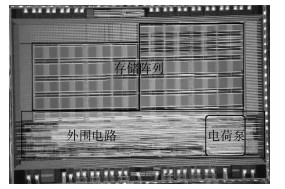
利用皮秒脉冲激光单粒子效应试验装置研究了一款宇航级Flash芯片的电流“尖峰”(HCS)现象。利用激光准确定位的特点,确定电流“尖峰”是由芯片的电荷泵单元充放电引起的,不同的激光能量、入射位置会触发不同频率、相同幅值的电流“尖峰”现象,虽然电流“尖峰”发生的瞬间电流增大的现象与单粒子锁定效应表现一致,但机理完全不同。当激光能量足够高(对应于重离子LET值99.8 MeV·cm2/mg)时,在电荷泵的同一个敏感位置累积多次辐照不断触发芯片发生电流“尖峰”,芯片会因多次充放电而损坏。
-
关键词:
- Flash芯片 /
- 电流“尖峰”(HCS) /
- 单粒子锁定 /
- 脉冲激光 /
- 电荷泵
Abstract:High Current Spike (HCS) of nonvolatile Flash chip has been tested by pico-second pulsed laser single event effect experimental facility. Accurate positioning of pulsed laser confirmed that sensitive area triggering HCS was charge pump of the chip. Different laser energies and specific locations in charge pump can trigger the same amplitude current spikes with different time cycle, although HCS has the same phenomenon with single event latch-up, and completely different mechanisms. When laser energy was high enough to be equivalent to heavy ion's LET value of 99.8 MeV·cm2/mg, continuous irradiation on the same sensitive area of charge pump can trigger the high current spike of the chip, which will cause catastrophic failure to the chip due to multiple charging and discharging.
-
Key words:
- Flash chip /
- High Current Spike (HCS) /
- single event latch-up /
- pulsed laser /
- charge pump
-

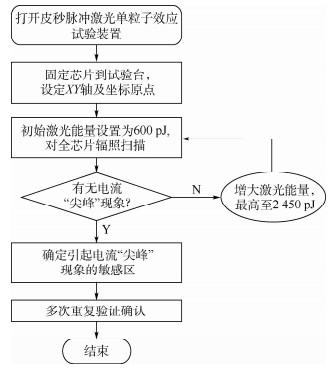
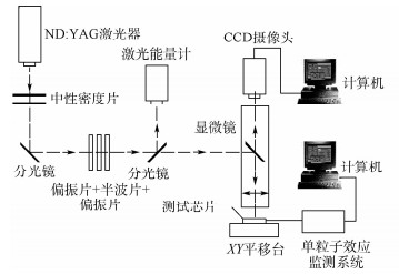
图 1 皮秒脉冲激光单粒子效应试验装置原理图
Figure 1. Schematic diagram of pico-second pulsed laser single event effect experimental facility

图 3 同一个位置HCS示波器不同显示分辨率的电流波形
Figure 3. Current waveform of same area caused HCS tested by different resolution of oscilloscope

图 5 不同激光能量下的芯片电流“尖峰”波形
Figure 5. Waveform of chip HCS caused by different laser energies
表 1 被测试芯片参数
Table 1. Tested chip parameters
类型 型号 厂商 质量等级 工艺尺寸 封装 工作电压 功耗电流 Flash芯片 YB29LV160 复旦微电子科技有限公司 宇航级 0.13 μm COB 3.3 V < 1 mA(静态)  下载: 导出CSV
-
[1] FAROKH I, NGUYEN D N. Single event effect characterization of high density commercial NAND and NOR nonvolatile flash memories[J]. IEEE Transactions on Nuclear Science, 2007, 54(6): 2547-2553. doi: 10.1109/TNS.2007.909984 [2] SHINDOU H, KUBOYAMA S, HIRAO T, et al. Local and pseudo SELs observed in digital LSIs and their implication to SEL test method[J]. IEEE Transactions on Nuclear Science, 2005, 52(6): 2638-2641. doi: 10.1109/TNS.2005.861081 [3] BI J S, XI K, LI B, et al. Heavy ion induced upset errors in 90-nm 64 Mb NOR-type floating-gate Flash memory[J]. Chinese Physics B, 2018, 27(9): 619-623. http://www.cnki.com.cn/Article/CJFDTotal-ZGWL201809089.htm [4] BAGATIN M, GERADIN S, PACCAGNELLA A, et al. Destructive events in NAND Flash memories irradiated with heavy ions[J]. Microelectronics Reliability, 2010, 50(5): 1832-1836. http://www.sciencedirect.com/science/article/pii/S0026271410003057 [5] FAROKH I, NGUYEN D, MARTA B S, et al. Catastrophic failure in highly scaled commercial NAND flash memories[J]. IEEE Transactions on Nuclear Science, 2010, 57(1): 266-271. doi: 10.1109/TNS.2009.2035315 [6] GERARDIN S, BAGATIN M, PACCAGNELLA A, et al. Investigation of supply current spikes in flash memories using ion-electron emission microscopy[J]. IEEE Transactions on Nuclear Science, 2013, 60(6): 4136-4141. doi: 10.1109/TNS.2013.2290012 [7] TIMOTHY R, OLDHAM M, FRIENDLICH R, et al. Correlation of laser test results with heavy ion results for NAND Flash memory[J]. IEEE Transactions on Nuclear Science, 2012, 59(6): 2831-2836. doi: 10.1109/TNS.2012.2222046 [8] 余永涛. 脉冲激光模拟SRAM单粒子效应的试验研究[D]. 北京: 中国科学院大学, 2015.YU Y T. Research of SRAM single event effects based on pulsed laser testing[D]. Beijing: University of Chinese Academy of Sciences, 2015(in Chinese). [9] 赵星, 梅博, 毕津顺, 等. 0.18μm部分耗尽绝缘体上硅互补金属氧化物半导体电路单粒子瞬态特性研究[J]. 物理学报, 2015, 64(13): 1-8. https://www.cnki.com.cn/Article/CJFDTOTAL-WLXB201513038.htmZHAO X, MEI B, BI J S, et al. Single event transients in a 0.18μm partially-depleted silicon-on-insulator complementary metal oxide semiconductor circuit[J]. Acta Physica Sinica, 2015, 64(13): 1-8(in Chinese). https://www.cnki.com.cn/Article/CJFDTOTAL-WLXB201513038.htm [10] CHEN R M, ZHANG F Q, CHEN W, et al. Single-event multiple transients in conventional and guard-ring hardened inverter chains under pulsed laser and heavy-ion irradiation[J]. IEEE Transaction on Nuclear Science, 2017, 64(9): 2511-2518. doi: 10.1109/TNS.2017.2738646 [11] SHANGGUAN S P, ZHU X, CHEN R, et al. Single event transient pulse width transmission of 0.13μm partial depleted SOI process DFF[J]. Journal of Beijing University of Aeronautics and Astronautics, 2019, 45(11): 2193-2198(in Chinese). http://en.cnki.com.cn/Article_en/CJFDTotal-BJHK201911009.htm [12] MA Y Q, HAN J W, FENG G Q, et al. Metallic layers reflections effects on the correlation of laser effective energy and heavy-ion LET for SEL testing[C]//Radiation Effects on Components and Systems (RADECS). Bremen: DE, 2016: 1-6. [13] MA Y Q, HAN J W, SHANGGUAN S P, et al. See characteristics of COTS devices by 1064 nm pulsed laser backside testing[C]//Proceedings of the 2018 IEEE Nuclear and Space Radiation Effects Conference. Piscataway: IEEE Press, 2018: 1-4. [14] 黄建国, 韩建伟. 脉冲激光模拟单粒子效应的等效LET计算[J]. 中国科学G辑: 物理学力学天文学, 2004, 34(6): 601-609. doi: 10.3969/j.issn.1674-7275.2004.06.001HUANG J G, HAN J W. Calculation of equivalent LET for pulsed laser simulating SEE[J]. Science in China Series G: Physics, Mechanics & Astronomy 2004, 34(6): 601-609(in Chinese). doi: 10.3969/j.issn.1674-7275.2004.06.001 [15] BI J S, ZENG C B, GAO L C, et al. Estimation of pulsed laser induced single event transient in a partially-depleted silicon-on-insulator 0.18μm MOSFET[J]. Chinese Physics B, 2014, 23(8): 1-5. http://www.cnki.com.cn/Article/CJFDTotal-ZGWL201408105.htm [16] 胡春媚, 陈书明, 吴振宇, 等. 利用脉冲激光的片上系统芯片单粒子效应试验[J]. 国防科技大学学报, 2017, 39(2): 134-139. https://www.cnki.com.cn/Article/CJFDTOTAL-GFKJ201702020.htmHU C M, CHEN S M, WU Z Y, et al. Single event effect experiment on SoC using pulsed laser[J]. Journal of National University of Defense Technology, 2017, 39(2): 134-139(in Chinese). https://www.cnki.com.cn/Article/CJFDTOTAL-GFKJ201702020.htm -

 下载:
下载:


 点击查看大图
计量
- 文章访问数: 646
- HTML全文浏览量: 225
- PDF下载量: 52
- 被引次数: 0
