


-
摘要:
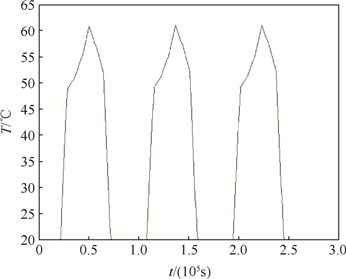
针对多数塑料焊球阵列(PBGA)封装芯片仅依据美军MIL标准进行高低温交变测试致使预测服役寿命偏差较大的情况,将微控制芯片任务状态时间谱转化为环境温度载荷谱,在综合考虑热传导、热对流的情形下,利用icepak完成芯片热电耦合仿真分析,并借助于Transient Thermal及Transient Structural完成芯片结温的获取及焊点应力、应变的计算求解。同时,依据Arrhenius模型及修正Coffin-Manson热疲劳模型分别预测芯片本身及焊点的寿命,从而实现对其热环境适应能力的定量分析。仿真结果表明:芯片的预测寿命约为6.26年,寿命预测偏差约为13.4%,符合GJB 4239-2001中单个关键环境因素预测寿命偏差标准,能够较为精确地反映其热环境适应性。
-
关键词:
- 塑料焊球阵列(PBGA)封装 /
- 芯片焊点 /
- 任务时间谱 /
- 热疲劳 /
- 环境适应性
Abstract:In view of the fact that most Plastic Ball Grid Array (PBGA) packaged chips are only subjected to high and low temperature alternating tests in accordance with the US military MIL standard, resulting in a large deviation in predicted service life, this paper converts the microcomputer control chip mission time spectrum into ambient temperature parameters, and comprehensively considers the heat conduction and heat convection, so as to use icepak to complete the chip thermoelectric coupling simulation analysis, and use Transient Thermal and Transient Structural to complete the chip junction temperature acquisition and solder joint stress and strain calculation and solution. At the same time, the life of chip itself and the solder joint are predicted based on the Arrhenius model and the modified Coffin-Manson thermal fatigue model, so as to realize the quantitative analysis of its thermal environment adaptability. The simulation results show that the predicted life of the chip is about 6.26 years, and the life prediction deviation is about 13.4%, which complies with GJB 4239's single key environmental factor predicted life deviation standard and accurately reflects its thermal environment adaptability.
-

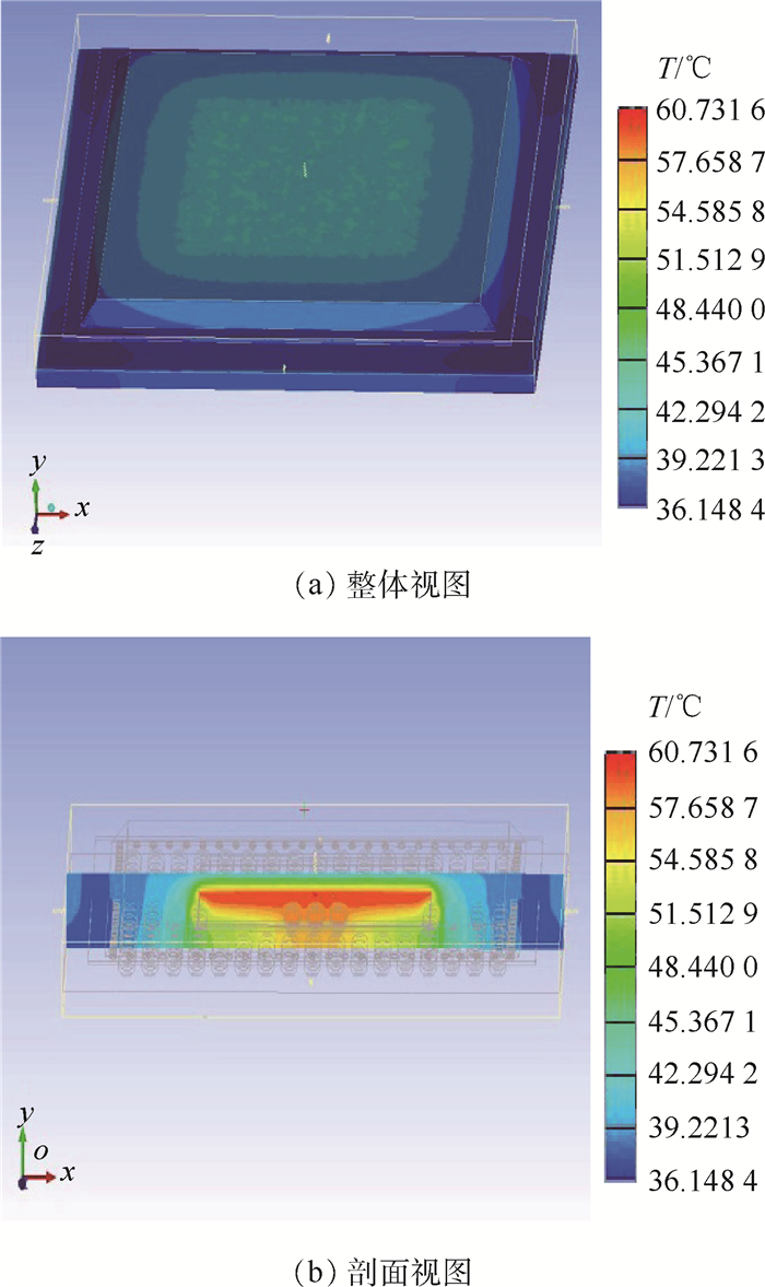
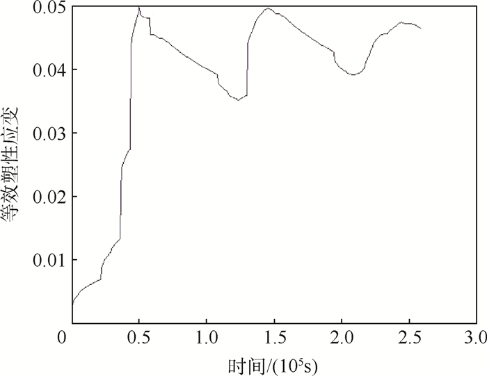
图 6 焊点等效塑性应变示意图
Figure 6. Schematic diagram of equivalent plastic strain of solder joint
表 1 芯片组成部分结构尺寸
Table 1. Chip component structure size
芯片结构 长度l/mm 宽度b/mm 厚度δ /mm 硅晶片 14 14 0.3 BT基板 27 27 0.15 黏结层 14 14 0.10 PCB板 30 30 1.0  下载: 导出CSV
表 2 材料热特性参数
Table 2. Thermal property parameters of material
零部件 材料 密度/ (kg·m-3) 比热容/ (J·(kg·K)-1) 热导率/ (W·(m·K)-1) 弹性模量/ MPa 泊松比 热膨胀系数/ K-1 裸芯片 Si 2 330 26+1.99T 180 162 716 0.28 1.3×10⁻⁵ 黏结层 环氧树脂 3 500 700 1.5 17 944-37.5T 0.35 * 基板 聚酰亚胺 1 700 880 0.33 24 132 0.30 1.6×10⁻⁵ 镀通孔 Cu 8 933 142+0.68T 387.6 128 932 0.34 1.7×10⁻⁵ PCB板 FR-4 1 900 750 0.2 22 000 0.28 1.9×10⁻⁵ 塑封 模塑树脂 1 900 800 0.7 68 220-150T 0.25 * 焊点 63Sn37Pb 8 470 150 51 75 842-152T 0.35 2.45×10⁻⁵ 注:“*”表示此处数值见表 3。
下载: 导出CSV
表 3 非线性热膨胀系数
Table 3. Nonlinear thermal expansion coefficient
温度/K 233 298 403 418 423 428 塑封热膨胀系数/K-1 9.0×10⁻⁶ 0 10-5 1.7×10⁻⁵ 2.2×10⁻⁵ 2.7×10⁻⁵ 温度/K 233 298 353 363 368 373 黏结层热膨胀系数/K-1 4.4×10⁻⁵ 0 4.5×10⁻⁵ 7.9×10⁻⁵ 8.9×10⁻⁵ 9.9×10⁻⁵
下载: 导出CSV
表 4 本构模型相关参数
Table 4. Relevant parameters of constitutive model
参数 数值 初始形变阻抗s0/MPa 56.33 激活能Q/(J·mol-1) 10 830 指数前系数因子A 1.49×10⁷ 应力因子ξ 11 应变硬化常数h0/MPa 2 640.75 应变率敏感指数m 0.303 形变阻抗饱和值系数 
80.415 应变率敏感度n 0.023 1 应变硬化指数α 1.34
下载: 导出CSV
表 5 加速退化试验样本数据
Table 5. Sample data of accelerated degradation test
样品序号 加速退化试验时间/h 退化量/% 预测寿命/h 1# 200 0.55 7 270.7 2# 200 0.58 6 896.6 3# 200 0.60 6 666.7 4# 300 0.83 7 228.9 5# 300 0.87 6 896.6 6# 300 0.80 7 500.0 7# 400 1.10 7 272.7 8# 400 1.09 7 339.4 9# 400 1.16 6 896.6 10# 500 1.40 7 142.9 11# 500 1.46 6 849.3 12# 500 1.48 6 756.8 13# 600 1.70 7 058.9 14# 600 1.73 6 936.4 15# 600 1.71 7 017.5
下载: 导出CSV
-
[1] JAYESH S, ELIAS J. Experimental and finite element analysis on determining the fatigue life of PB-free solder joint (Sn-0.5Cu-3Bi-1Ag) used in electronic packages under harmonic loads[J]. International Journal of Modeling, Simulation, and Scientific Computing, 2020, 11(3): 2050020. [2] FAHIM A, HASAN K, AHMED S, et al. Mechanical behavior evolution of SAC305 lead free solder joints under thermal cycling[C]//2019 18th IEEE Intersociety Conference on Thermal and Thermomechanical Phenomena in Electronic Systems (ITherm). Piscataway: IEEE Press, 2019, 5: 734-744. [3] 李志强, 马世辉, 飞尚才, 等. 热冲击条件下倒装焊点失效的有限元模拟[J]. 热加工工艺, 2018, 47(19): 233-236. https://www.cnki.com.cn/Article/CJFDTOTAL-SJGY201819064.htmLI Z Q, MA S H, FEI S C, et al. Finite element simulation of failure of flip chip solder joint under thermal shock[J]. Hot Working Technology, 2018, 47(19): 233-236(in Chinese). https://www.cnki.com.cn/Article/CJFDTOTAL-SJGY201819064.htm [4] U.S. Department of Defense. Reliability prediction of electronic equipment: MIL-HDBK-217F[S]. Washingtion, D.C. : U.S. Department of Defense, 2015: 48-53. [5] 陈镜波, 何小琦, 章晓文. 厚膜DC/DC电源VDMOS器件失效机理及研究现状[J]. 半导体技术, 2010, 35(2): 176-180. doi: 10.3969/j.issn.1003-353x.2010.02.020CHEN J B, HE X Q, ZHANG X W. Progress and failure mechanism of VDMOS device in DC/DC power supply[J]. Semiconductor Technology, 2010, 35(2): 176-180(in Chinese). doi: 10.3969/j.issn.1003-353x.2010.02.020 [6] KARVAN P, VARVANI-FARAHANI A. Viscoplastic ratcheting response of materials under step-loading conditions at various cyclic stress levels[J]. Journal of Materials Engineering and Performance, 2020, 29(2): 1124-1134. doi: 10.1007/s11665-020-04628-w [7] 焦鸿浩. 多物理场载荷下电子封装板级焊点仿真研究[D]. 哈尔滨: 哈尔滨理工大学, 2019: 25-32.JIAO H H. Simulation research on electronic package board level solder joint under multiphysics load[D]. Harbin: Harbin University of Science and Technology, 2019: 25-32(in Chinese). [8] TSAI S T, LIN C Y, WU S M, et al. Analyses and statistics of the electrical fail for flip chip packaging by using ANSYS simulation software and really underfill materials[J]. Microsystem Technologies, 2018, 24(10): 4017-4024. doi: 10.1007/s00542-017-3605-4 [9] LONG X, CHEN Z B, WANG W J, et al. Parameterized Anand constitutive model under a wide range of temperature and strain rate: Experimental and theoretical studies[J]. Journal of Materials Science, 2020, 55(24): 10811-10823. doi: 10.1007/s10853-020-04689-1 [10] 田野. 热冲击条件下倒装组装微焊点的可靠性-应力应变[J]. 焊接学报, 2016, 37(8): 67-70. https://www.cnki.com.cn/Article/CJFDTOTAL-HJXB201608016.htmTIAN Y. Micro-joint reliability of flip chip assembly under thermal shock-strain and stress[J]. Transactions of the China Welding Institution, 2016, 37(8): 67-70(in Chinese). https://www.cnki.com.cn/Article/CJFDTOTAL-HJXB201608016.htm [11] ENJU J, TRUNG N H, FADZLI S K, et al. Design and fabrication of on-chip micro-thermoelectric cooler based on electrodeposition process[J]. IEEJ Transactions on Sensors and Micromachines, 2020, 140(1): 18-23. doi: 10.1541/ieejsmas.140.18 [12] 应保胜, 刘冬冬, 吴华伟, 等. 基于Icepak的多种间隙下IGBT散热器仿真与研究[J]. 重庆交通大学学报(自然科学版), 2020, 39(2): 132-137. https://www.cnki.com.cn/Article/CJFDTOTAL-CQJT202002020.htmYING B S, LIU D D, WU H W, et al. Simulation and research of IGBT radiator under multiple gaps based on Icepak[J]. Journal of Chongqing Jiaotong University (Natural Science), 2020, 39(2): 132-137(in Chinese). https://www.cnki.com.cn/Article/CJFDTOTAL-CQJT202002020.htm [13] 连兴峰, 苏继龙. 封装热效应及粘结层对微芯片应力和应变的影响[J]. 机电技术, 2012, 35(6): 33-36. https://www.cnki.com.cn/Article/CJFDTOTAL-JDJS201206013.htmLIAN X F, SU J L. The influence of package thermal effect and adhesive layer on microchip stress and strain[J]. Mechanical & Electrical Technology, 2012, 35(6): 33-36(in Chinese). https://www.cnki.com.cn/Article/CJFDTOTAL-JDJS201206013.htm [14] 朱楠. 功率半导体模块电、热特性分析及应用[D]. 杭州: 浙江大学, 2018: 32-35.ZHU N. Electrical and thermal analysis and applications of power semiconductor modules[D]. Hangzhou: Zhejiang University, 2018: 32-35(in Chinese). [15] SOMAN V, VENKATADRI V, POLIKS M D. Understanding the effects of process parameters to compensate for substrate warpage in chip on flex (CoF) assembly using conventional reflow[J]. International Symposium on Microelectronics, 2019, 2019(1): 428-433. doi: 10.4071/2380-4505-2019.1.000428 [16] TAN S H, HAN J, WANG Y, et al. A method to determine the slip systems in BGA lead-free solder joints during thermal fatigue[J]. Journal of Materials Science: Materials in Electronics, 2018, 29(9): 7501-7509. doi: 10.1007/s10854-018-8741-9 [17] 田野, 任宁. 热冲击条件下倒装组装微焊点的可靠性-寿命预测[J]. 焊接学报, 2016, 37(2): 51-54. https://www.cnki.com.cn/Article/CJFDTOTAL-HJXB201602013.htmTIAN Y, REN N. Prediction of reliability of solder joint for fine pitch flip chip assemblies under thermal shock[J]. Transactions of the China Welding Institution, 2016, 37(2): 51-54(in Chinese). https://www.cnki.com.cn/Article/CJFDTOTAL-HJXB201602013.htm [18] 吕卫民, 李永强. 电子功能部件环境适应性试验优化设计[J]. 系统工程与电子技术, 2020, 42(7): 1630-1636. https://www.cnki.com.cn/Article/CJFDTOTAL-XTYD202007028.htmLYU W M, LI Y Q. Electronic functional equipment environmental adaptability test optimal design[J]. Systems Engineering and Electronics, 2020, 42(7): 1630-1636(in Chinese). https://www.cnki.com.cn/Article/CJFDTOTAL-XTYD202007028.htm [19] LI J L, TIAN Y B, WANG D P. Change-point detection of failure mechanism for electronic devices based on Arrhenius model[J]. Applied Mathematical Modelling, 2020, 83: 46-58. http://www.sciencedirect.com/science/article/pii/S0307904X20300962 [20] 郭小辉. 无铅钎料在PCB再流焊中翘曲的模拟仿真[D]. 天津: 天津大学, 2007: 15-18.GUO X H. Simulation for lead-free solder in the reflow welding of PCB warpage deformation[D]. Tianjin: Tianjin University, 2007: 15-18(in Chinese). [21] LIBOT J B, ALEXIS J, DALVERNY O, et al. Experimental SAC305 shear stress-strain hysteresis loop construction using Hall's one-dimensional model based on strain gages measurements[J]. Journal of Electronic Packaging, 2019, 141(2): 136-142. http://www.onacademic.com/detail/journal_1000041629555099_fda1.html [22] 中国人民解放军总装备部. 装备环境工程通用要求: GJB 4239-2001[S]. 北京: 中国人民解放军总装备部, 2001: 10-13.Chinese People's Liberation Army General Armament Department. General requirements for equipment environmental engineering: GJB 4239-2001[S]. Beijing: Chinese People's Liberation Army General Armament Department, 2001: 10-13(in Chinese). [23] 张卫. 考虑多失效机理耦合的电子产品寿命预测方法研究[D]. 长沙: 国防科学技术大学, 2014: 26-35.ZHANG W. Research on life prediction method of electronic product combined multiple-failure mechanism[D]. Changsha: National University of Defense Technology, 2014: 26-35(in Chinese). -

 下载:
下载:


 点击查看大图

计量
- 文章访问数: 446
- HTML全文浏览量: 123
- PDF下载量: 92
- 被引次数: 0
