| Citation: | GUO Chuncheng, HAO Xudan, CHEN Feiet al. Design of a novel read and write assisted circuit in low power SRAM[J]. Journal of Beijing University of Aeronautics and Astronautics, 2020, 46(8): 1618-1624. doi: 10.13700/j.bh.1001-5965.2019.0533(in Chinese)

|
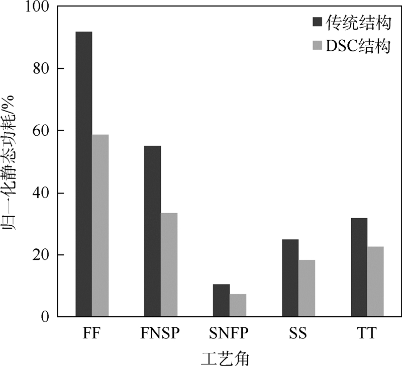
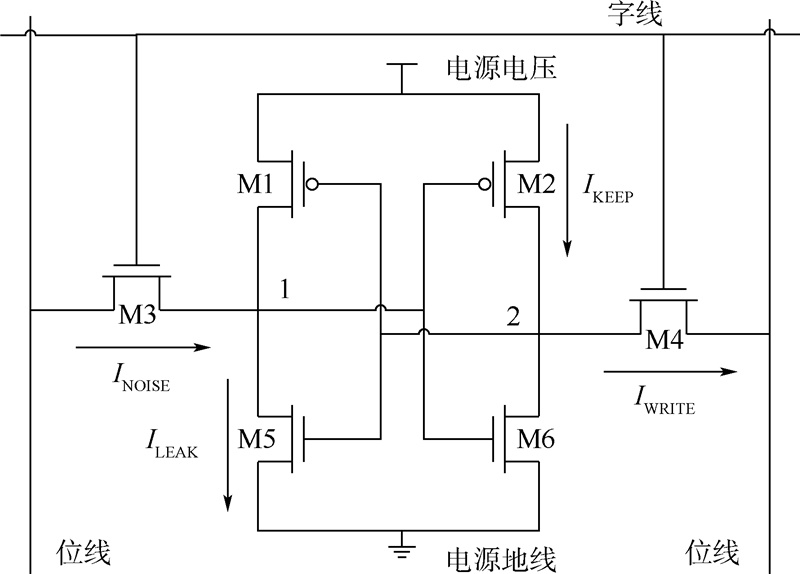
In order to solve the problem of read and write performance loss in Static Random-Access Memory (SRAM) under low voltage, a novel Dual-Step Control (DSC) word-line voltage technique for low power SRAM is designed, which can simultaneously realize read and write performance and reduce the minimum operation voltage of SRAM. Thus the power consumed is reduced. Write-assist implementation uses the Word-Line Over Drive (WLOD) at the beginning of the word-line to reduce the write access time and improve Write Margin (WM). And read-assist implementation uses the Word-Line Under Drive (WLUD) after the WLOD to reduce static noise and increase the stability. A 256 Kbit SRAM pre-sim and post-sim simulation, which is designed in 28 nanometer Complementary Metal Oxide Semiconductor (CMOS) process, demonstrates that DSC-SRAM lowers the minimum operation voltage by 100 mV, reduces the write access time by 10%, decreases the static power by 30%, and increases its layout area by 4%, compared to the conventional SRAM structure.

| [1] |
MARINISSEN E J, PRINCE B, KEITEL-SCHULZ D, et al.Challenges in embedded memory design and test[C]//Proceedings of Design, Automation and Test in Europe.Piscataway: IEEE Press, 2005: 722-727.
|
| [2] |
ZHANG K.Embedded memories for nano-scale VLSIs[M].Berlin:Springer, 2009:91-93.
|
| [3] |
BHASKAR A.Design and analysis of low power SRAM cells[C]//2017 Innovations in Power and Advanced Computing Technologies.Piscataway: IEEE Press, 2018: 1-5.
|
| [4] |
TAKASHIMA D, ENDO M, SHIMAZAKI K, et al.A 7T-SRAM with data-write technique by capacitive coupling[J].IEEE Journal of Solid-State Circuits, 2019, 54(2):596-605. doi: 10.1109/JSSC.2018.2875108
|
| [5] |
GROVER A, VISWESWARAN G S, PARTHASARATHY C R, et al.A 32 kb 0.35-1.2 V, 50 MHz-2.5 GHz bit-interleaved SRAM with 8T SRAM cell and data dependent write assist in 28 nm UTBB-FDSOI CMOS[J].IEEE Transactions on Circuits and Systems I:Regular Papers, 2017, 64(9):2438-2447. doi: 10.1109/TCSI.2017.2705116
|
| [6] |
SAXENA S, MEHRA R.Low-power and high-speed 13T SRAM cell using FinFETs[J].IET Circuits Devices & Systems, 2017, 11(3):250-255. http://www.wanfangdata.com.cn/details/detail.do?_type=perio&id=133a489b36da39859e25b1e9ca51aa66
|
| [7] |
DUAN C, GOTTERBA A J, SINANGIL M E, et al.Energy-efficient reconfigurable SRAM:Reducing read power through data statistics[J].IEEE Journal of Solid-State Circuits, 2017, 52(10):1-9. doi: 10.1109/JSSC.2017.2741663
|
| [8] |
PAVLOV A.CMOS SRAM circuit design and parametric test in nano-scaled technologies[M].Berlin:Springer, 2008:2703-2711.
|
| [9] |
NHO H, KOLAR P, HAMZAOGLU F, et al.A 32 nm high-k metal gate SRAM with adaptive dynamic stability enhancement for low-voltage operation[C]//IEEE International Solid-State Circuits Conference.Piscataway: IEEE Press, 2010: 76-84.
|
| [10] |
SONG T, RIM W, PARK S, et al.A 10 nm FinFET 128 Mb SRAM with assist adjustment system for power, performance, and area optimization[J].IEEE Journal of Solid-State Circuits, 2017, 52(1):240-249. doi: 10.1109/JSSC.2016.2609386
|
| [11] |
LIEN N C, CHU L W, CHEN C H, et al.A 40 nm 512 kb cross-point 8T pipeline SRAM with binary word-line boosting control, ripple bit-line and adaptive data-aware write-assist[J].IEEE Transactions on Circuits and Systems I:Regular Papers, 2017, 61(12):3416-3425. http://www.wanfangdata.com.cn/details/detail.do?_type=perio&id=7fa8856e3e9ba3e94a0a2e17149c51fe
|
| [12] |
CHEN Y H, CHAN W M, WU W C, et al.A 16 nm 128 Mb SRAM in high-k metal-gate FinFET technology with write-assist circuitry for low-VMIN applications[J].IEEE Journal of Solid-State Circuits, 2015, 50(1):170-177. doi: 10.1109/JSSC.2014.2349977
|
| [13] |
SINANGIL M E, POULTON J W, FOJTIK M R, et al.A 28 nm 2 Mbit 6T SRAM with highly configurable low-voltage write-ability assist implementation and capacitor-based sense-amplifier input offset compensation[J].IEEE Journal of Solid-State Circuits, 2015, 50(2):557-567. http://www.wanfangdata.com.cn/details/detail.do?_type=perio&id=73fddc8b1cf2fbfaa025f37ab1b83c24
|
| [14] |
CHANG M F, CHEN C F, CHANG T H, et al.A compact-area low-VDDmin 6T SRAM with improvement in cell stability, read speed, and write margin using a dual-split-control-assist scheme[J].IEEE Journal of Solid-State Circuits, 2017, 52(9):2498-2514. doi: 10.1109/JSSC.2017.2701547
|
| [15] |
SINANGIL M E, MAIR H, CHANDRAKASAN A P.A 28 nm high-density 6T SRAM with optimized peripheral-assist circuits for operation down to 0.6V[C]//IEEE International Solid-State Circuits Conference.Piscataway: IEEE Press, 2011: 260-261.
|
Figures(10) / Tables(1)
Copyright © Journal of Beijing University of Aeronautics and Astronautics
Address: Editorial Department of Journal of Beijing University of Aeronautics and Astronautics, 37 Xueyuan Road, Haidian District, Beijing Post Code: 100191 Email: jbuaa@buaa.edu.cn
Supported by:
Beijing Renhe Information Technology Co., Ltd.


 DownLoad: