| Citation: | LI Sai, CHEN Rui, HAN Jianweiet al. Single-event-transient pulse width characteristics of 130 nm bulk silicon inverter chain[J]. Journal of Beijing University of Aeronautics and Astronautics, 2019, 45(6): 1137-1144. doi: 10.13700/j.bh.1001-5965.2018.0568(in Chinese)

|
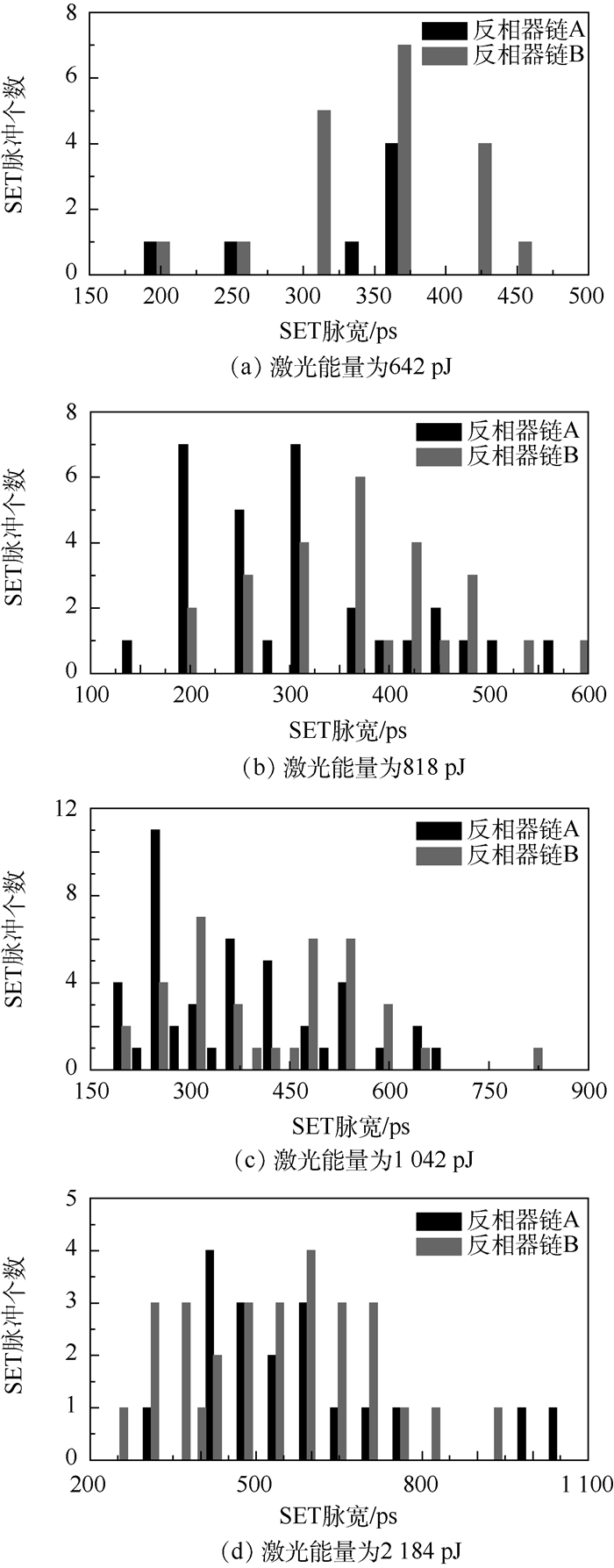
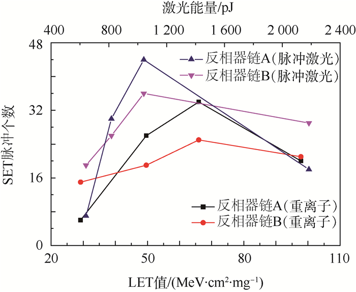
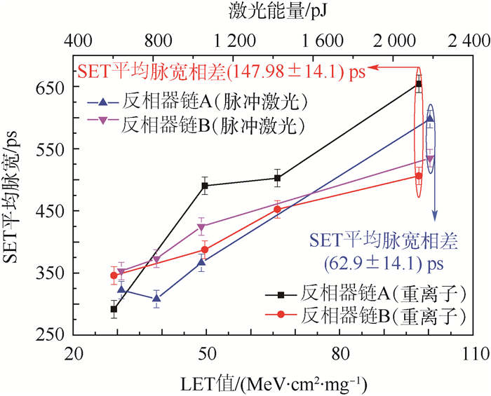
Experimental research of single-event-transient (SET) is carried out by means of pulse laser and heavy ion irradiation on the inverter chain fabricated by 130 nm bulk silicon process. The impacts of laser energy, heavy ion linear energy transfer (LET), and PMOS gate length on the characteristics of SET pulse width were analyzed. Experimental results of heavy ion and laser are similar, and both results show that the pulse width of SET increases with laser energy/LET raise, and the distribution of SET pulse width has double (or multiple) peaks, but the number of SET generated in the circuit increases first and then decreases. In addition, the experimental results show that, under different laser energy/LET, the size of PMOS gate length affects the characteristics of SET differently. At low laser energy/LET, the circuit with larger PMOS gate length produces a wider SET pulse, and on the contrary, at high laser energy/LET, the circuit with smaller PMOS gate length produces a wider SET pulse. Through the analysis of the experimental results, it is found that the parasitic bipolar amplification effect may be the main cause of the difference of SET characteristics with high energy/LET irradiation.

| [1] |
ECOFFET R.Overview of in-orbit radiation induced spacecraft anomalies[J].IEEE Transaction on Nuclear Science, 2013, 60(3):1791-1815. doi: 10.1109/TNS.2013.2262002
|
| [2] |
FERLET-CAVROIS V, MASSENGILL L W, GOUKER P.Single event transients in digital CMOS-A review[J].IEEE Transaction on Nuclear Science, 2013, 60(3):1767-1790. doi: 10.1109/TNS.2013.2255624
|
| [3] |
LIU J B, LIU Y, CHENG J L, et al.Simulations of single event transient effects in the LM139 voltage comparator[C]//International Conference on Reliability, Maintainability and Safety.Piscataway, NJ: IEEE Press, 2014: 189-192.
|
| [4] |
REN Y, CHEN L, SHI S T, et al.Single-event transient measurement on a DC/DC PWM controller using pulsed X-ray technique[C]//IEEE International Reliability Physics Symposium. Piscataway, NJ: IEEE Press, 2013: SE.3.1-SE.3.5.
|
| [5] |
DU Y K, CHEN S M.A novel layout-based single event transient injection approach to evaluate the soft error rate of large combinational circuits in complimentary metal-oxide-semiconductor bulk technology[J].IEEE Transactions on Reliability, 2016, 65(1):248-255. doi: 10.1109/TR.2015.2427372
|
| [6] |
ANDJELKOVIC M, KRSTIC M, KRAEMER R.Comparison of the SET sensitivity of standard logic gates designed in 130 nm CMOS technology[C]//International Conference on Microelectronics. Piscataway, NJ: IEEE Press, 2017: 217-220.
|
| [7] |
ANDJELKOVIC M, ILIC A, PETROVIC V, et al.SET response of a SEL protection switch for 130 and 250 nm CMOS technologies[C]//IEEE International Symposium on On-Line Testing and Robust System Design. Piscataway, NJ: IEEE Press, 2016: 185-190.
|
| [8] |
DURGA G, BALAMURUGAN V, SRINIVASAN R.Single event transient analysis on junctionless silicon nanotube field effect transistor[C]//International Conference on Information Communication and Embeded Systems. Piscataway, NJ: IEEE Press, 2017: 1-4.
|
| [9] |
陈睿, 余永涛, 上官士鹏, 等.90 nm互补金属氧化物半导体静态随机存储器局部单粒子闩锁传播效应诱发多位翻转的机理[J].物理学报, 2014, 63(12):128501. http://d.old.wanfangdata.com.cn/Periodical/wlxb201412054
CHEN R, YU Y T, SHANGGUAN S P, et al.Mechanism of multiple bit upsets induced by localized latch-up effect in 90 nm complementary metal semiconductor static random-access memory[J].Acta Physica Sinica, 2014, 63(12):128501(in Chinese). http://d.old.wanfangdata.com.cn/Periodical/wlxb201412054
|
| [10] |
DARRACQ F, LAPUYADE H, BUARD N, et al.Backside SEU laser testing for commercial-off-the-shelf SRAMs[J].IEEE Transactions on Nuclear Science, 2002, 49(6):2977-2983. doi: 10.1109/TNS.2002.805393
|
| [11] |
FERLET-CAVROIS V, PAILLET P, GAILLARDIN M.Statistical analysis of the charge collected in SOI and bulk devices under heavy ion and proton irradiation-Implications for digital SETs[J].IEEE Transaction on Nuclear Science, 2006, 53(6):3242-3252. doi: 10.1109/TNS.2006.885111
|
| [12] |
CHEN S M, LIANG B.Temperature dependence of digital SET pulse width in bulk and SOI technologies[J].IEEE Transaction on Nuclear Science, 2008, 55(6):2914-2920. doi: 10.1109/TNS.2008.2006980
|
| [13] |
CHEN R M, ZHANG F Q, CHEN W, et al.Single-event multiple transients in conventional and guard-ring hardened inverter chains under pulsed laser and heavy-ion irradiation[J].IEEE Transactions on Nuclear Science, 2017, 64(9):2511-2518. doi: 10.1109/TNS.2017.2738646
|
| [14] |
AMUSAN O A, MASSENGILL L W, BHUVA B L, et al.Design techniques to reduce SET pulse widths in deep-submicron combinational logic[J].IEEE Transaction on Nuclear Science, 2007, 54(6):2060-2064. doi: 10.1109/TNS.2007.907754
|
| [15] |
GADLAGE M J, AHLBIN J R, NARASIMHAM B, et al.Single-event transient measurements in nMOS and pMOS transistors in a 65 nm bulk CMOS technology at elevated temperatures[J].IEEE Transactions on Device and Materials Reliability, 2011, 11(2):179-186.
|
| [16] |
JAGANNATHAN S, GADLAGE M J, BHUVA B L, et al.Independent measurement of SET pulse widths from N-hits and P-hits in 65 nm CMOS[J].IEEE Transactions on Nuclear Science, 2010, 57(6):3386-3391. http://www.wanfangdata.com.cn/details/detail.do?_type=perio&id=13a19d377b1a459662b628bf803a8e91
|
| [17] |
AMUSAN O A, WITULSKI A F, MASSENGILL L W, et al.Charge collection and charge sharing in a 130 nm CMOS technology[J].IEEE Transactions on Nuclear Science, 2006, 53(6):3253-3258. doi: 10.1109/TNS.2006.884788
|
| [18] |
刘家齐, 赵元富, 王亮, 等.65 nm反相器单粒子瞬态脉宽的多峰值现象[J].微电子技术, 2017, 43(1):20-23. http://www.wanfangdata.com.cn/details/detail.do?_type=perio&id=dzjsyy201701007
LIU J Q, ZHAO Y F, WANG L, et al.The multi-peak phenomenon in 65 nm inverters single event transient pulse width distribution[J].Microelectronic Technology, 2017, 43(1):20-23(in Chinese). http://www.wanfangdata.com.cn/details/detail.do?_type=perio&id=dzjsyy201701007
|
| [19] |
OLSON B D, BALL D R, WARREN K W, et al.Simultaneous single event charge sharing and parasitic bipolar conduction in a high-scaled SRAM design[J].IEEE Transaction on Nuclear Science, 2005, 52(6):2132-2136. doi: 10.1109/TNS.2005.860684
|
| [20] |
刘蓉容, 池雅庆, 窦强.结深对65 nm体硅CMOS晶体管单粒子瞬态脉冲的影响[J].计算机工程与科学, 2017, 39(12):2176-2184. http://www.wanfangdata.com.cn/details/detail.do?_type=perio&id=jsjgcykx201712003
LIU R R, CHI Y Q, DOU Q.Impact of junction depth on SET pulse width in 65 nm bulk CMOS transistor[J].Computer Engineering and Science, 2017, 39(12):2176-2184(in Chinese). http://www.wanfangdata.com.cn/details/detail.do?_type=perio&id=jsjgcykx201712003
|
| [21] |
刘征, 陈书明, 梁斌, 等.单粒子瞬变中的双极放大效应研究[J].物理学报, 2010, 59(1):649-654. http://d.old.wanfangdata.com.cn/Periodical/wlxb201001106
LIU Z, CHEN S M, LIANG B, et al.Research of bipolar amplification effect in single event transient[J].Acta Physica Sinica, 2010, 59(1):649-654(in Chinese). http://d.old.wanfangdata.com.cn/Periodical/wlxb201001106
|
| [22] |
FERLET-CAVROIS V, PAILLET P, MCMORROW D, et al.Direct measurement of transient pulses induced by laser and heavy ion irradiation in deca-nanometer devices[J].IEEE Transactions on Nuclear Science, 2005, 52(6):2104-2113. doi: 10.1109/TNS.2005.860682
|
| [23] |
DODD P E, SEXTON F W, HASH G L, et al.Impact of technology trends on SEU in CMOS SRAMs[J].IEEE Transactions on Nuclear Science, 1996, 43(6):2797-2804. doi: 10.1109/23.556869
|
| [24] |
薛玉雄, 曹洲, 杨世宇, 等.重离子和脉冲激光模拟单粒子翻转阈值等等效性研究[J].原子能科学技术, 2007, 41(6):653-658. http://www.wanfangdata.com.cn/details/detail.do?_type=perio&id=yznkxjs200706004
XUE Y X, CAO Z, YANG S Y, et al.Equivalence study on heavy ion and pulsed laser simulation of single-event upset threshold[J].Atomic Energy Science and Technology, 2007, 41(6):653-658(in Chinese). http://www.wanfangdata.com.cn/details/detail.do?_type=perio&id=yznkxjs200706004
|
| [25] |
JOHNSTON A H.Charge generation and collection in p-n junctions excited with pulsed infrared[J].IEEE Transactions on Nuclear Science, 1993, 40(6):1694-1702. doi: 10.1109/23.273491
|
| [26] |
RAINE M, HUBERT G, GAILLARDIN M, et al. Impact of the radial ionization profile on see prediction for SOI transistors and SRAMs beyond the 32 nm technological node[J]. IEEE Transactions on Nuclear Science, 2011, 58(3):840-847. doi: 10.1109/TNS.2011.2109966
|

Figures(7) / Tables(1)
Copyright © Journal of Beijing University of Aeronautics and Astronautics
Address: Editorial Department of Journal of Beijing University of Aeronautics and Astronautics, 37 Xueyuan Road, Haidian District, Beijing Post Code: 100191 Email: jbuaa@buaa.edu.cn
Supported by:
Beijing Renhe Information Technology Co., Ltd.


 DownLoad: