| Citation: | DANG Yanjie, LIANG Yu, ZHANG Weiet al. Design of a new path-sharing true-time-delay beamformer architecture[J]. Journal of Beijing University of Aeronautics and Astronautics, 2019, 45(6): 1266-1272. doi: 10.13700/j.bh.1001-5965.2018.0626(in Chinese)

|
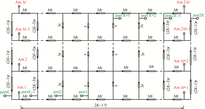
In order to meet the requirement of multi-input and multi-output of broadband wireless communication system, a new path-sharing true-time-delay beamformer architecture is proposed in this paper. The output capability is improved by synthesizing multiple signals, compensating the time difference in reaching the antenna with a certain delay difference provided by the true-time-delay unit. Compared with the traditional beamformer architecture, this architecture can save the area of chip by true-time-delay unit sharing. It is not only extensional, supporting 2

| [1] |
DUATRE V C, DRUMMOND M V, NOGUEIRA R N.Coherent photonic true-time-delay beamforming system for a phased array antenna receiver[C]//International Conference on Transparent Optical Networks.Piscataway, NJ: IEEE Press, 2016: 1-5. https://ieeexplore.ieee.org/document/7550663
|
| [2] |
MOSLLRMI S, WELKER R, KITCHEN J.Wide band programmable true time delay block for phased array antenna applications[C]//Dallas Circuits and Systems Conference.Piscataway, NJ: IEEE Press, 2017. https://ieeexplore.ieee.org/document/7847754
|
| [3] |
肖永轩, 薛永, 曾小金.GEO移动通信卫星合成多波束天线仿真分析[J].航天器工程, 2010, 19(3):74-79. doi: 10.3969/j.issn.1673-8748.2010.03.011
XIAO Y X, XUE Y, ZENG X J.Simulation analysis of composite multi-beam antenna on the GEO mobile communication satellite[J].Spacecraft Engineering, 2010, 19(3):74-79(in Chinese). doi: 10.3969/j.issn.1673-8748.2010.03.011
|
| [4] |
MOALLEMI S, WELKER R, KITCHEN J.Wide band programmable true time delay block for phased array antenna applications[C]//Dallas Circuits and Systems Conference.Piscataway, NJ: IEEE Press, 2017. https://ieeexplore.ieee.org/document/7847754
|
| [5] |
AHMADI P, BELOSTOTSKI L, MADANAYAKE A, et al.0.96-to-5.1GHz 4-element spatially analog IIR-enhanced delay-and-sum beamformer[C]//International Microwave Symposium.Piscataway, NJ: IEEE Press, 2017: 1610-1613. https://ieeexplore.ieee.org/document/8058942
|
| [6] |
LIU Y, ZHANG W, LIU Y.A fully integrated 4-channel beamformer based on TTD phased array in 0.18μm CMOS[J].Microelectronics Journal, 2018, 80:81-86. doi: 10.1016/j.mejo.2018.07.003
|
| [7] |
ARIYARATHNA V, UDAYANGA N, MADANAYAKE A, et al.Design methodology of an analog 9-beam squint-free wideband IF multi-beamformer for mmW applications[C]//Moratuwa Engineering Research Conference.Piscataway, NJ: IEEE Press, 2017: 236-240. https://ieeexplore.ieee.org/document/7980488
|
| [8] |
高浩, 周以国, 郭征.L波段宽带相控阵天线真延时网络的设计[J].电子元件与材料, 2013, 32(6):14-17. doi: 10.3969/j.issn.1001-2028.2013.06.004
GAO H, ZHOU Y G, GUO Z.Design of a true time delay network for the L-band wideband phased array antenna[J].Electronic Components and Materials, 2013, 32(6):14-17(in Chinese). doi: 10.3969/j.issn.1001-2028.2013.06.004
|
| [9] |
CHU T S, RODERICK J, HASHEMI H.An integrated ultra-wideband timed array receiver in 0.13μm CMOS using a path-sharing true time delay architecture[J].IEEE Journal of Solid-State Circuits, 2007, 42(12):2834-2850. doi: 10.1109/JSSC.2007.908746
|
| [10] |
CHU T S, HASHEMI H.A CMOS UWB camera with 7×7 simultaneous active pixels[C]//International Solid-State Circuits Conference-Digest of Technical Papers.Piscataway, NJ: IEEE Press, 2008: 120-121. https://ieeexplore.ieee.org/document/4523086
|
| [11] |
CHU T S, HASHEMI H.True-time-delay-based multi-beam arrays[J].IEEE Transactions on Microwave Theory & Techniques, 2013, 61(8):3072-3082. http://d.old.wanfangdata.com.cn/NSTLQK/NSTL_QKJJ0230602086/
|
| [12] |
CHU T S, HASHEMI H.A true time-delay-based bandpass multi-beam array at mm-waves supporting instantaneously wide bandwidths[C]//International Solid-State Circuits Conference.Piscataway, NJ: IEEE Press, 2010: 38-39. https://ieeexplore.ieee.org/document/5434060
|
| [13] |
MA L, WANG Z, XU J, et al.A 500 kHz-1.4 GHz push-pull differential noise cancellation LNA[C]//IEEE International Conference on Communication Software and Networks.Piscataway, NJ: IEEE Press, 2015: 182-185. https://ieeexplore.ieee.org/document/7296150
|
| [14] |
BRUCCOLERI F, KLUMPERINK E A M, NAUTA B.Wide-band CMOS low-noise amplifier exploiting thermal noise canceling[J].IEEE Journal of Solid-State Circuits, 2004, 39(2):275-282. doi: 10.1109/JSSC.2003.821786
|
| [15] |
邵翔鹏, 张万荣, 丁春宝, 等.基于噪声抵消技术的超宽带低噪声放大器[J].电子器件, 2015(1):74-77. doi: 10.3969/j.issn.1005-9490.2015.01.017
SHAO X P, ZHANG W R, DING C B, et al.An ultra-wideband low noise amplifier based on noise cancellation technique[J].Chinese Journal of Electron Devices, 2015(1):74-77(in Chinese). doi: 10.3969/j.issn.1005-9490.2015.01.017
|
| [16] |
MONDAL I, KRISHNAPURA N.A 2 GHz bandwidth, 0.25~1.7 ns true-time-delay element using a variable-order all-pass filter architecture in 0.13μm CMOS[J].IEEE Journal of Solid-State Circuits, 2017, 52(8):2180-2193. doi: 10.1109/JSSC.2017.2693229
|
| [17] |
GARAKOUI S K, KLUMPERINK E A M, NAUTA B, et al.Compact cascadable gm-C all-pass true time delay cell with reduced delay variation over frequency[J].IEEE Journal of Solid-State Circuits, 2015, 50(3):693-703. doi: 10.1109/JSSC.2015.2390214
|

Figures(13) / Tables(1)
Copyright © Journal of Beijing University of Aeronautics and Astronautics
Address: Editorial Department of Journal of Beijing University of Aeronautics and Astronautics, 37 Xueyuan Road, Haidian District, Beijing Post Code: 100191 Email: jbuaa@buaa.edu.cn
Supported by:
Beijing Renhe Information Technology Co., Ltd.


 DownLoad: