| Citation: | SHI Z,WANG B,YANG B,et al. Single-event radiation hardening method for 14 nm pFinFET device[J]. Journal of Beijing University of Aeronautics and Astronautics,2023,49(12):3335-3342 (in Chinese) doi: 10.13700/j.bh.1001-5965.2022.0071

|
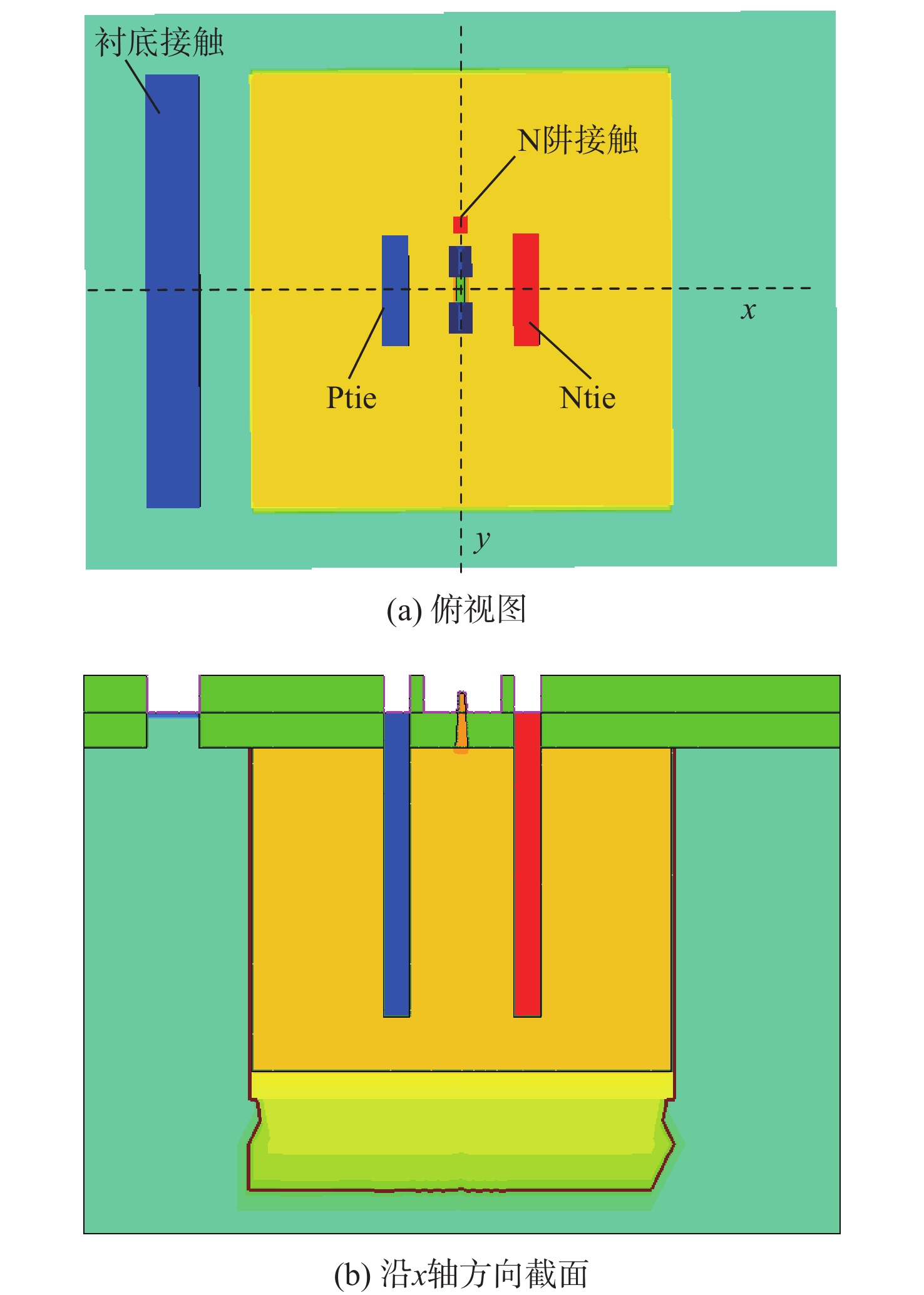
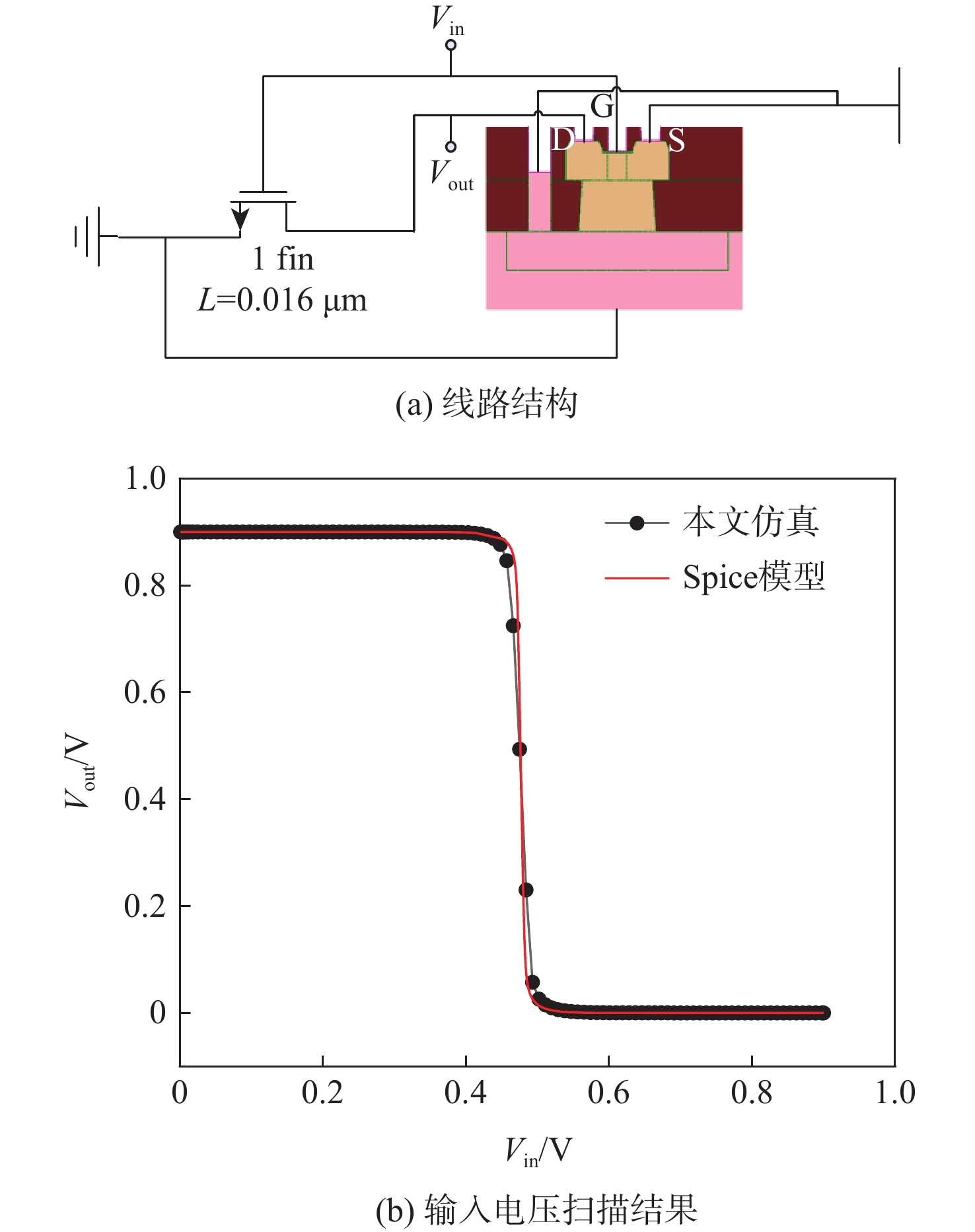
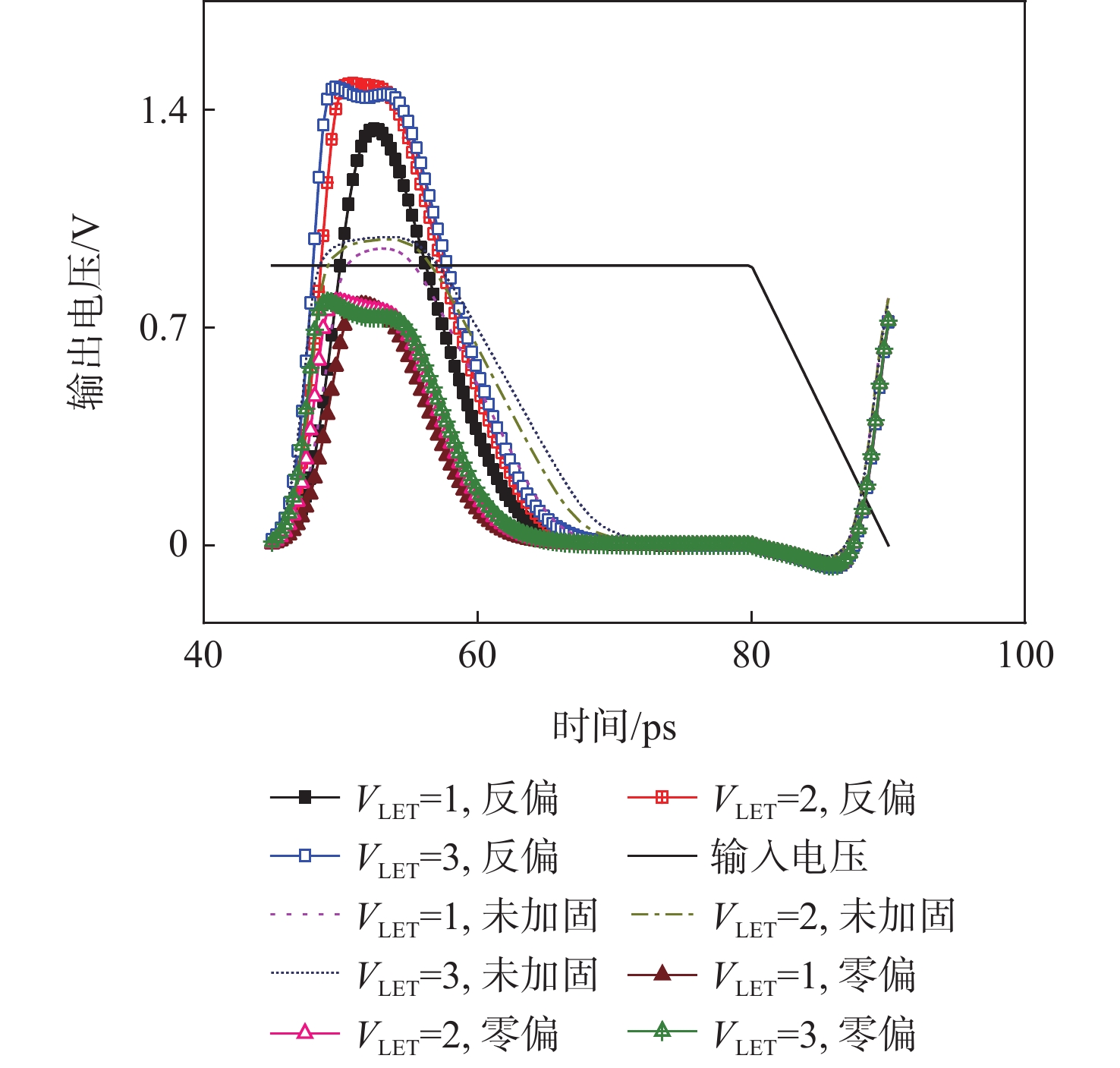
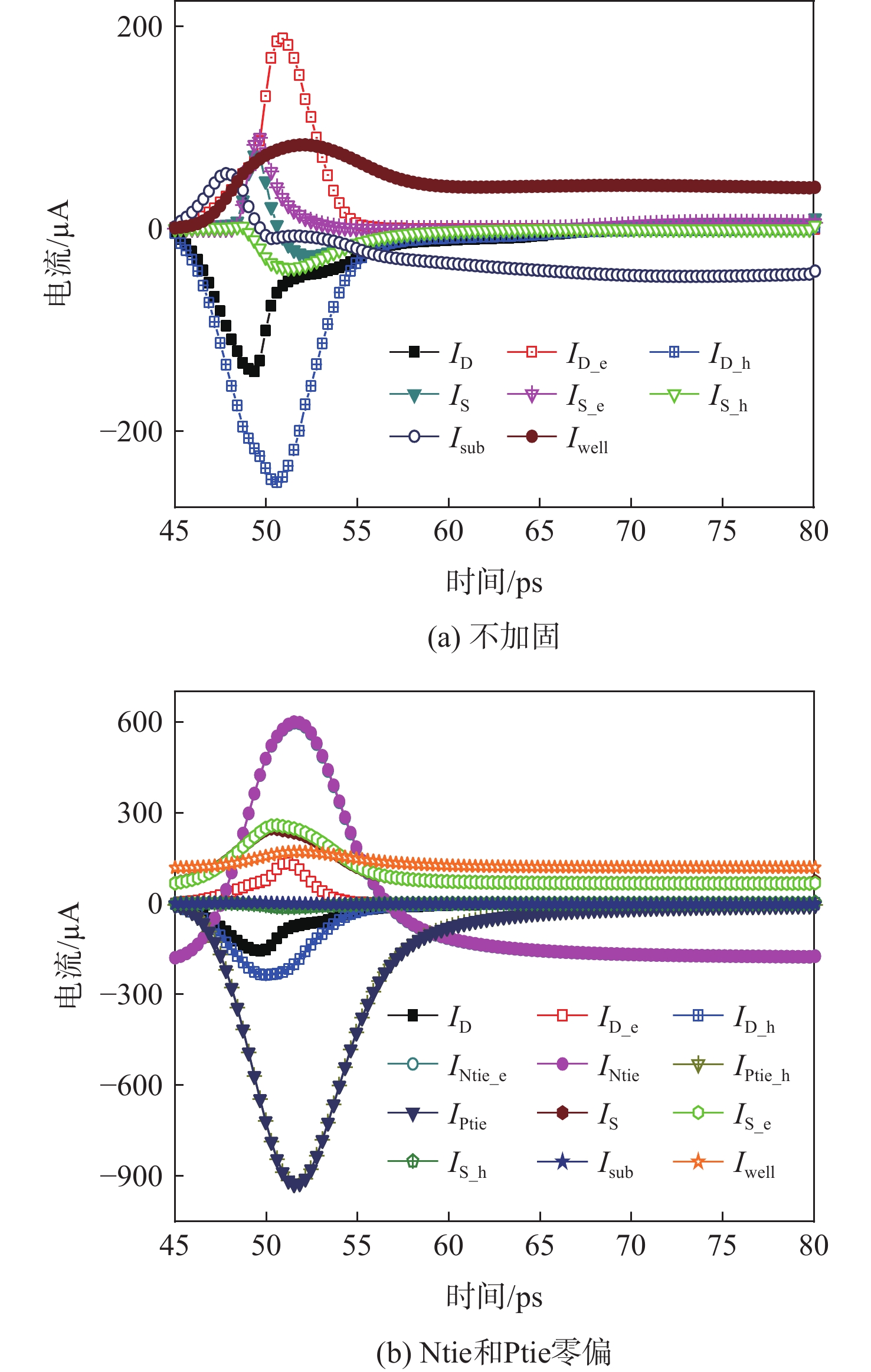
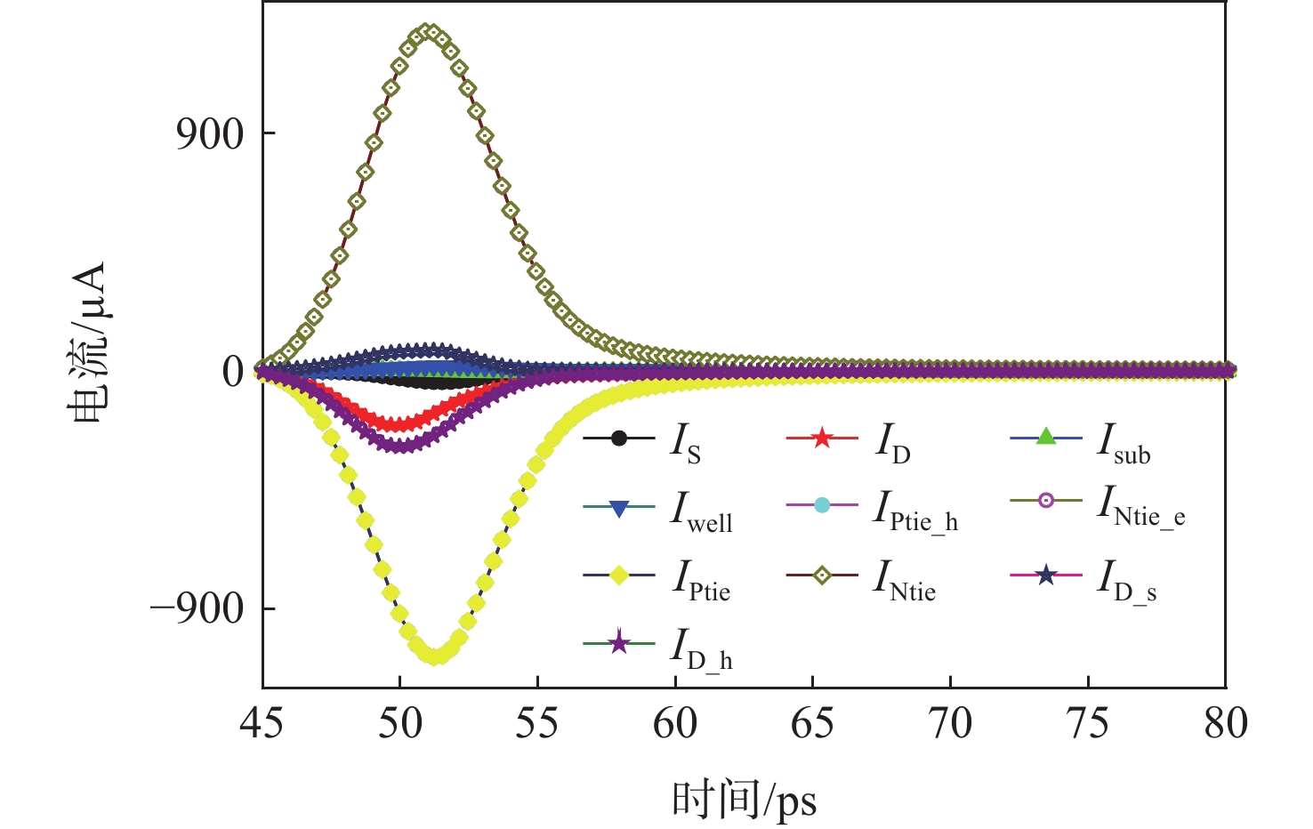
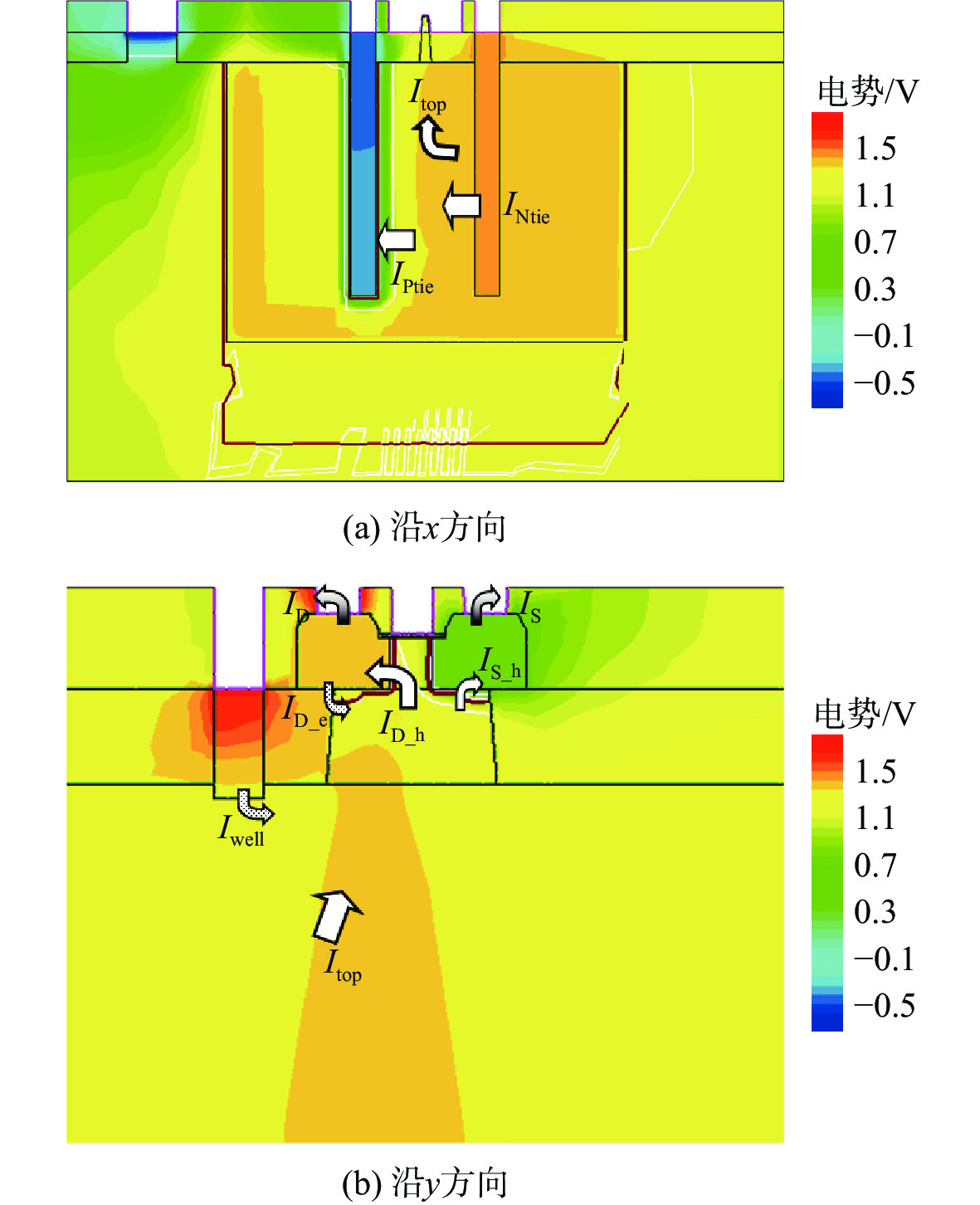
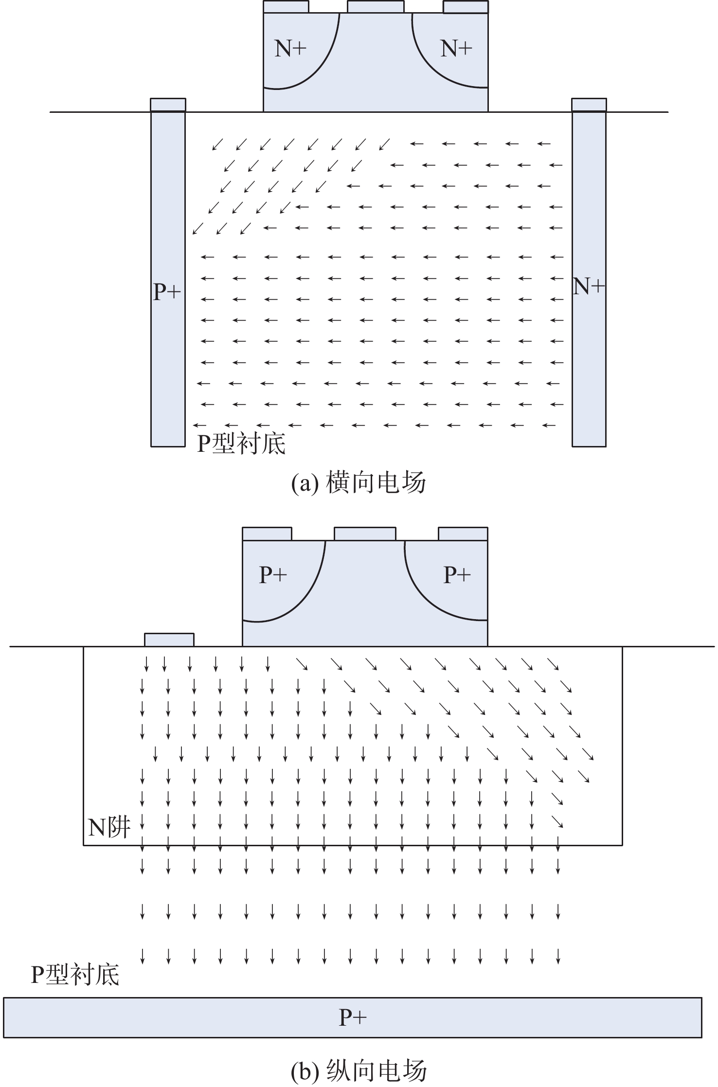
In order to investigate the reliability of advanced complementary metal-oxide-semiconductor (CMOS) processes for space applications, a hardening strategy against single-event transient (SET) is investigated in P-channel fin field-effect transistor (pFinFET) devices at 14 nm. The effects of SETs are mitigated by inserting heavily doped N-type trenches (Ntie) and P-type trenches (Ptie) parallel to the fin direction in the device. Three-dimensional TCAD simulations show that the resistance to SET of the device by introducing trenches is related to the bias conditions of the trenches themselves. The SET voltage pulse amplitude increases significantly when the trenches are in the reverse-bias state due to the presence of a special charge collection process, in addition to a slight decrease in pulse width compared to the unhardened devices, which results in the best radiation-hardening performance when the trenches are at zero bias and have a reduction in SET pulse width of about 40%. Besides, the impact of trench area, spacing, and doping concentration on the SET pulse width in the pFinFET is also investigated, obtaining the device parameters with the best resistance to SET.

| [1] |
SEIFERT N, JAHINUZZAMAN S, VELAMALA J, et al. Soft error rate improvements in 14-nm technology featuring second-generation 3D tri-gate transistors[J]. IEEE Transactions on Nuclear Science, 2015, 62(6): 2570-2577. doi: 10.1109/TNS.2015.2495130
|
| [2] |
YI B, LEE B J, OH J H, et al. Physics-based compact model of parasitic bipolar transistor for single-event transients in FinFETs[J]. IEEE Transactions on Nuclear Science, 2018, 65(3): 866-870. doi: 10.1109/TNS.2018.2796622
|
| [3] |
NSENGIYUMVA P, MASSENGILL L W, KAUPPILA J S, et al. Angular effects on single-event mechanisms in bulk FinFET technologies[J]. IEEE Transactions on Nuclear Science, 2018, 65(1): 223-230. doi: 10.1109/TNS.2017.2775234
|
| [4] |
KUMAR S, CHO M, EVERSON L, et al. Analysis of neutron-induced multibit-upset clusters in a 14-nm flip-flop array[J]. IEEE Transactions on Nuclear Science, 2019, 66(6): 918-925. doi: 10.1109/TNS.2019.2911540
|
| [5] |
JIANG H, ZHANG H, CHATTERJEE I, et al. Power-aware SE analysis of different FF designs at the 14-16-nm bulk FinFET CMOS technology node[J]. IEEE Transactions on Nuclear Science, 2018, 65(8): 1866-1871. doi: 10.1109/TNS.2018.2831002
|
| [6] |
CALOMARDE A, AMAT E, RUBIO A, et al. Active charge collection strategy for radiation environment at device level[C]//2016 16th European Conference on Radiation and Its Effects on Components and Systems. Piscataway: IEEE Press, 2017: 1-4.
|
| [7] |
SANDEEPAN D G. Trends in single event pulse widths and pulse shapes in deep submicron CMOS[D]. Nashville: Vanderbilt University, 2007: 45-50.
|
| [8] |
CALOMARDE A, RUBIO A, MOLL F, et al. Active radiation-hardening strategy in bulk FinFETs[J]. IEEE Access, 2020, 8: 201441-201449. doi: 10.1109/ACCESS.2020.3035974
|
| [9] |
AMUSAN O A, MASSENGILL L W, BHUVA B L, et al. Design techniques to reduce SET pulse widths in deep-submicron combinational logic[J]. IEEE Transactions on Nuclear Science, 2007, 54(6): 2060-2064. doi: 10.1109/TNS.2007.907754
|
| [10] |
JAGANNATHAN S, GADLAGE M J, BHUVA B L, et al. Independent measurement of SET pulse widths from N-hits and P-hits in 65-nm CMOS[J]. IEEE Transactions on Nuclear Science, 2010, 57(6): 3386-3391.
|
| [11] |
ZHAO W, HE C H, CHEN W, et al. Single-event double transients in inverter chains designed with different transistor widths[J]. IEEE Transactions on Nuclear Science, 2019, 66(7): 1491-1499. doi: 10.1109/TNS.2019.2895610
|
| [12] |
史柱, 赵雁鹏, 高利军, 等. 抗单粒子瞬态的辐射加固压控延时单元[J]. 西安交通大学学报, 2021, 55(9): 105-112.
SHI Z, ZHAO Y P, GAO L J, et al. A radiation-hardened voltage-controlled delay cell against single-event-transient[J]. Journal of Xi’an Jiaotong University, 2021, 55(9): 105-112 (in Chinese).
|
| [13] |
王琳, 宋李梅, 王立新, 等. 一种提升抗单粒子能力的新型超结结构[J]. 微电子学与计算机, 2019, 36(9): 84-88. doi: 10.19304/j.cnki.issn1000-7180.2019.09.016
WANG L, SONG L M, WANG L X, et al. A proposed structure to improve SEE performance for 700 V Super-Junction VDMOS[J]. Microelectronics & Computer, 2019, 36(9): 84-88(in Chinese). doi: 10.19304/j.cnki.issn1000-7180.2019.09.016
|
| [14] |
董刚, 封国强, 陈睿, 等. CMOS器件单粒子效应电荷收集机理[J]. 北京航空航天大学学报, 2014, 40(6): 839-843. doi: 10.13700/j.bh.1001-5965.2013.0435
DONG G, FENG G Q, CHEN R, et al. Single event charge collection in CMOS device[J]. Journal of Beijing University of Aeronautics and Astronautics, 2014, 40(6): 839-843(in Chinese). doi: 10.13700/j.bh.1001-5965.2013.0435
|
| [15] |
EL-MAMOUNI F, ZHANG E X, PATE N D, et al. Laser- and heavy ion-induced charge collection in bulk FinFETs[J]. IEEE Transactions on Nuclear Science, 2011, 58(6): 2563-2569. doi: 10.1109/TNS.2011.2171994
|
| [16] |
MUNTEANU D, AUTRAN J L. Simulation analysis of bipolar amplification in independent-gate FinFET and multi-channel NWFET submitted to heavy-ion irradiation[J]. IEEE Transactions on Nuclear Science, 2012, 59(6): 3249-3257. doi: 10.1109/TNS.2012.2221740
|
| [17] |
FERLET-CAVROIS V, PAILLET P, MCMORROW D, et al. Direct measurement of transient pulses induced by laser and heavy ion irradiation in deca-nanometer devices[J]. IEEE Transactions on Nuclear Science, 2005, 52(6): 2104-2113. doi: 10.1109/TNS.2005.860682
|
| [18] |
鄂长江, 李少甫, 齐艺轲. 单粒子多瞬态诱导的组合电路软错误敏感性评估[J]. 微电子学与计算机, 2019, 36(11): 16-19. doi: 10.19304/j.cnki.issn1000-7180.2019.11.004
E C J, LI S F, QI Y K. Soft error sensitivity estimation of single event multi-transient induced combination circuits[J]. Microelectronics & Computer, 2019, 36(11): 16-19(in Chinese). doi: 10.19304/j.cnki.issn1000-7180.2019.11.004
|
| [19] |
MAHARREY J A, KAUPPILA J S, HARRINGTON R C, et al. Impact of single-event transient duration and electrical delay at reduced supply voltages on SET mitigation techniques[J]. IEEE Transactions on Nuclear Science, 2018, 65(1): 362-368. doi: 10.1109/TNS.2017.2779818
|
| [20] |
ZHANG H F, JIANG H, ASSIS T R, et al. Single-event upset responses of dual- and triple-well designs at advanced planar and FinFET technologies[C]//2016 16th European Conference on Radiation and Its Effects on Components and Systems. Piscataway: IEEE Press, 2017: 1-6.
|
| [21] |
NSENGIYUMVA P, MASSENGILL L W, ALLES M L, et al. Analysis of bulk FinFET structural effects on single-event cross sections[J]. IEEE Transactions on Nuclear Science, 2017, 64(1): 441-448. doi: 10.1109/TNS.2016.2620940
|
| [22] |
DING L L, CHEN W, WANG T, et al. Modeling the dependence of single-event transients on strike location for circuit-level simulation[J]. IEEE Transactions on Nuclear Science, 2019, 66(6): 866-874. doi: 10.1109/TNS.2019.2904716
|
| [23] |
AMUSAN O A, MASSENGILL L W, BAZE M P, et al. Mitigation techniques for single-event-induced charge sharing in a 90-nm bulk CMOS process[J]. IEEE Transactions on Device and Materials Reliability, 2009, 9(2): 311-317. doi: 10.1109/TDMR.2009.2019963
|
| [24] |
YU J T, CHEN S M, CHEN J J, et al. Simulation analysis of heavy-ion-induced single-event response for nanoscale bulk-Si FinFETs and conventional planar devices[J]. Science China Technological Sciences, 2017, 60(3): 459-466. doi: 10.1007/s11431-016-0241-4
|
Figures(8) / Tables(2)
Copyright © Journal of Beijing University of Aeronautics and Astronautics
Address: Editorial Department of Journal of Beijing University of Aeronautics and Astronautics, 37 Xueyuan Road, Haidian District, Beijing Post Code: 100191 Email: jbuaa@buaa.edu.cn
Supported by:
Beijing Renhe Information Technology Co., Ltd.


 DownLoad: