


Based on on-chip real-time monitoring with adaptive compensation for anti-total dose bandgap reference
-
摘要:
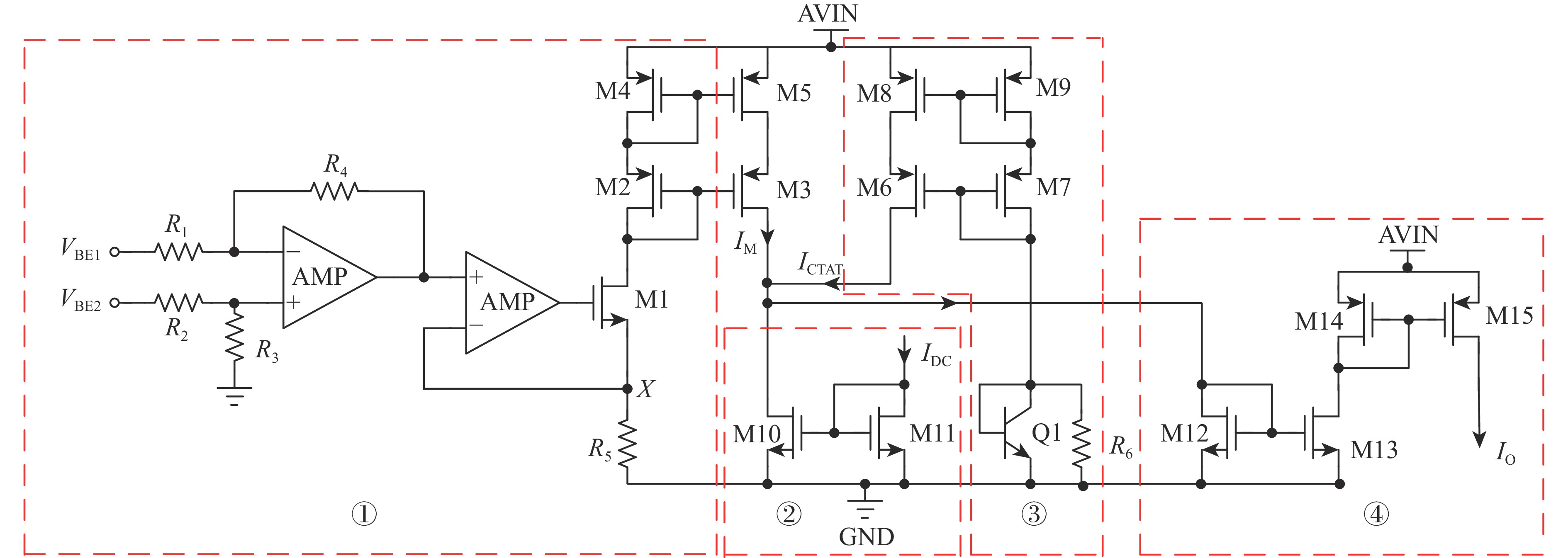
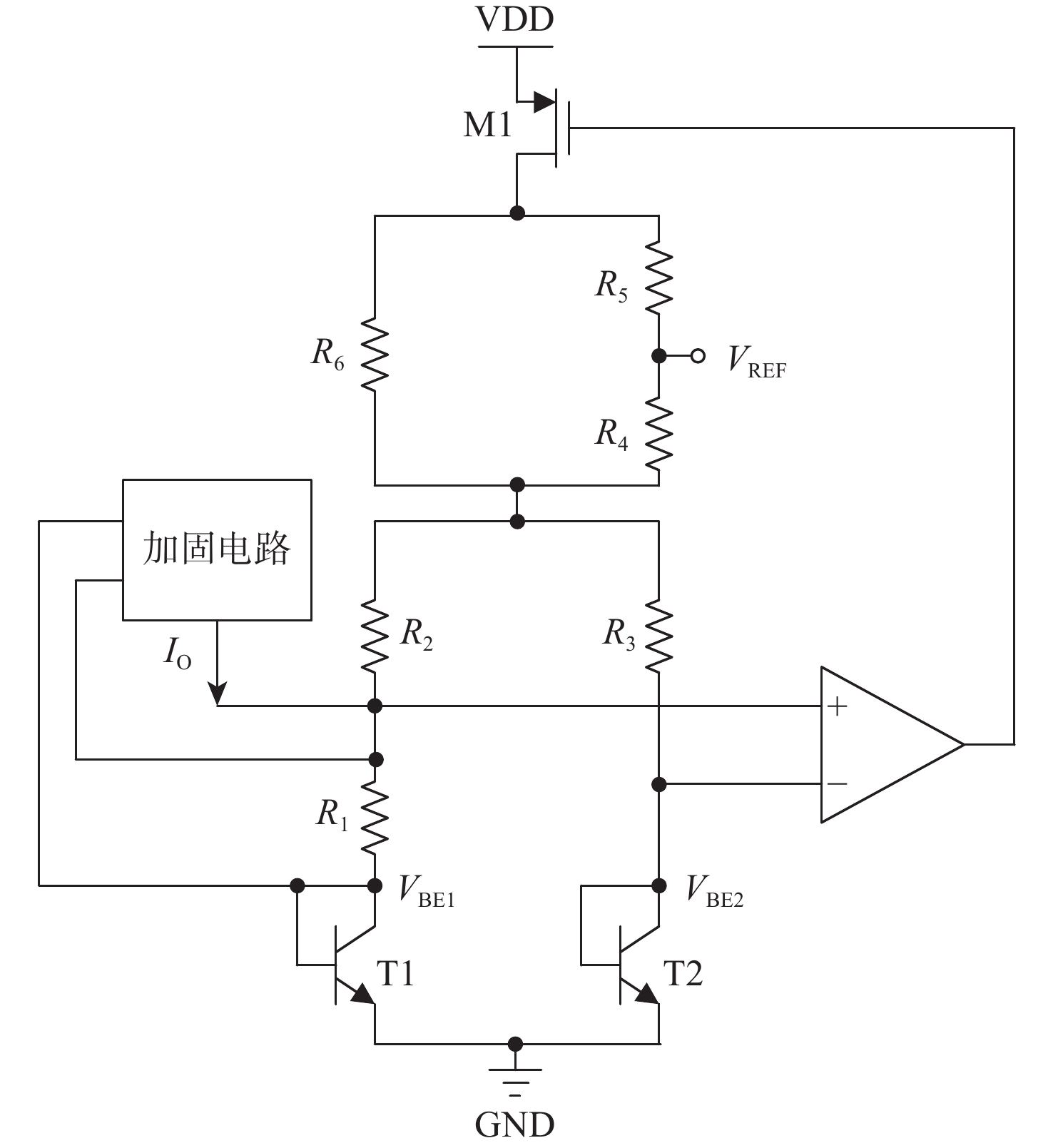
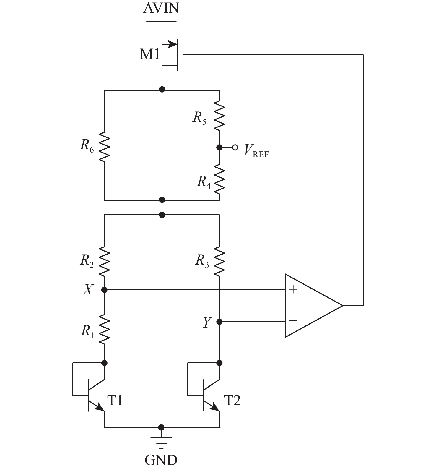
带隙基准电路在总剂量辐射环境下会出现双极晶体管基极电流泄漏,电流增益下降,从而造成带隙基准输出电压偏移,使得带隙基准的可靠性下降。针对传统带隙基准基于工艺、版图和器件的总剂量加固方法会带来的成本过高、版图面积过大、普适性不高等问题,提出一种片上总剂量实时监测与自适应补偿方法,实现电路级的总剂量加固,提高了带隙基准的抗辐射能力。基于0.18 μm BCD工艺对所提方法进行具体电路设计、后端物理实现与全面验证,结果表明:不同工艺角下,分别在总剂量辐照为100~300 krad (Si)辐射条件下,带隙基准的输出电压偏移由加固前偏移电压为3.4~18.5 mV (100~300 krad)改善为加固后最大偏移电压为1 mV (100~300 krad),为电路与系统级的带隙基准抗辐照加固设计提供了一种新方法。
Abstract:Bipolar transistor base current leakage and a drop in current gain will occur in bandgap reference circuits exposed to total dose radiation. This will cause the output voltage of the bandgap reference to move and its dependability to decline. To address the issues of high cost, large layout area, and low universality that traditional total dose reinforcement methods for bandgap references based on process, layout, and device can bring, this method is suggested. An on-chip total dose real-time monitoring and adaptive compensation method is proposed to realize circuit-level total dose reinforcement and improve the radiation resistance of bandgap references. Based on the 0.18 μm BCD (Bipolar-CMOS-DMOS) process, specific circuit design, back-end physical implementation and comprehensive verification of the proposed method are carried out. Under radiation conditions of 100−300 krad (Si) under various process angles, the results demonstrate that the output voltage offset of the bandgap reference is improved from 3.4−18.5 mV voltage offset (100−300 krad) prior to reinforcement to the maximum offset voltage following reinforcement, which is 1 mV (100−300 krad). This provides a new method for designing irradiation-resistant reinforcement of bandgap references at the circuit and system levels.
-
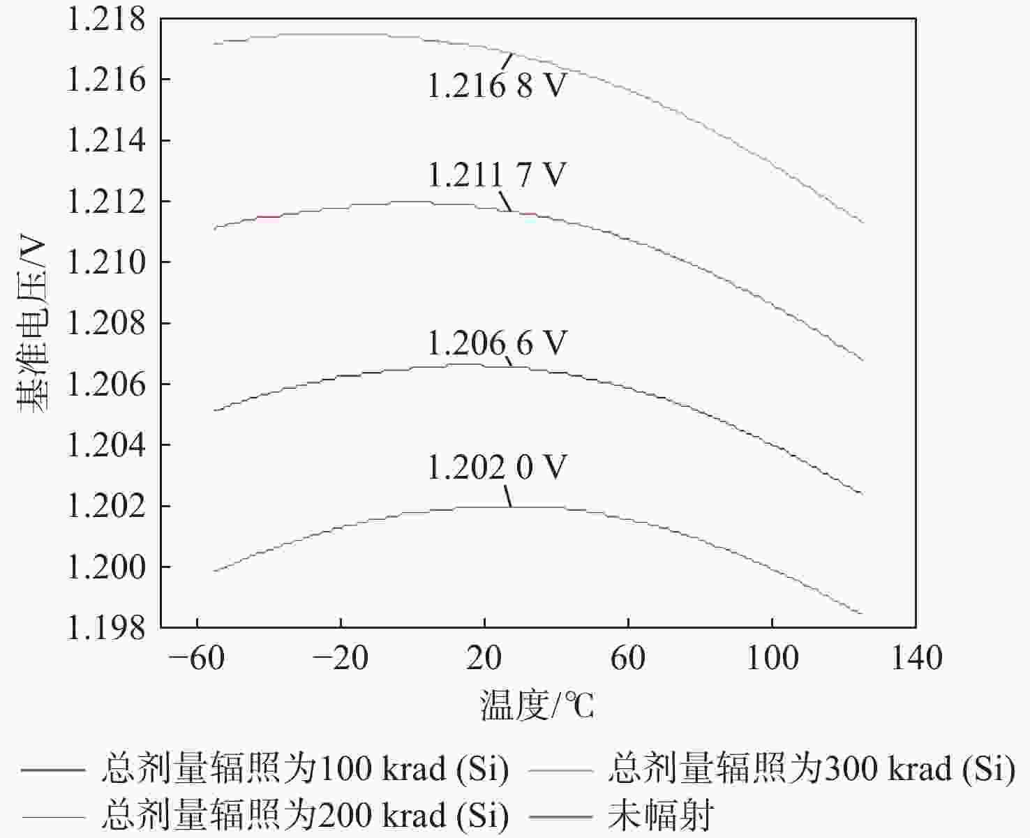
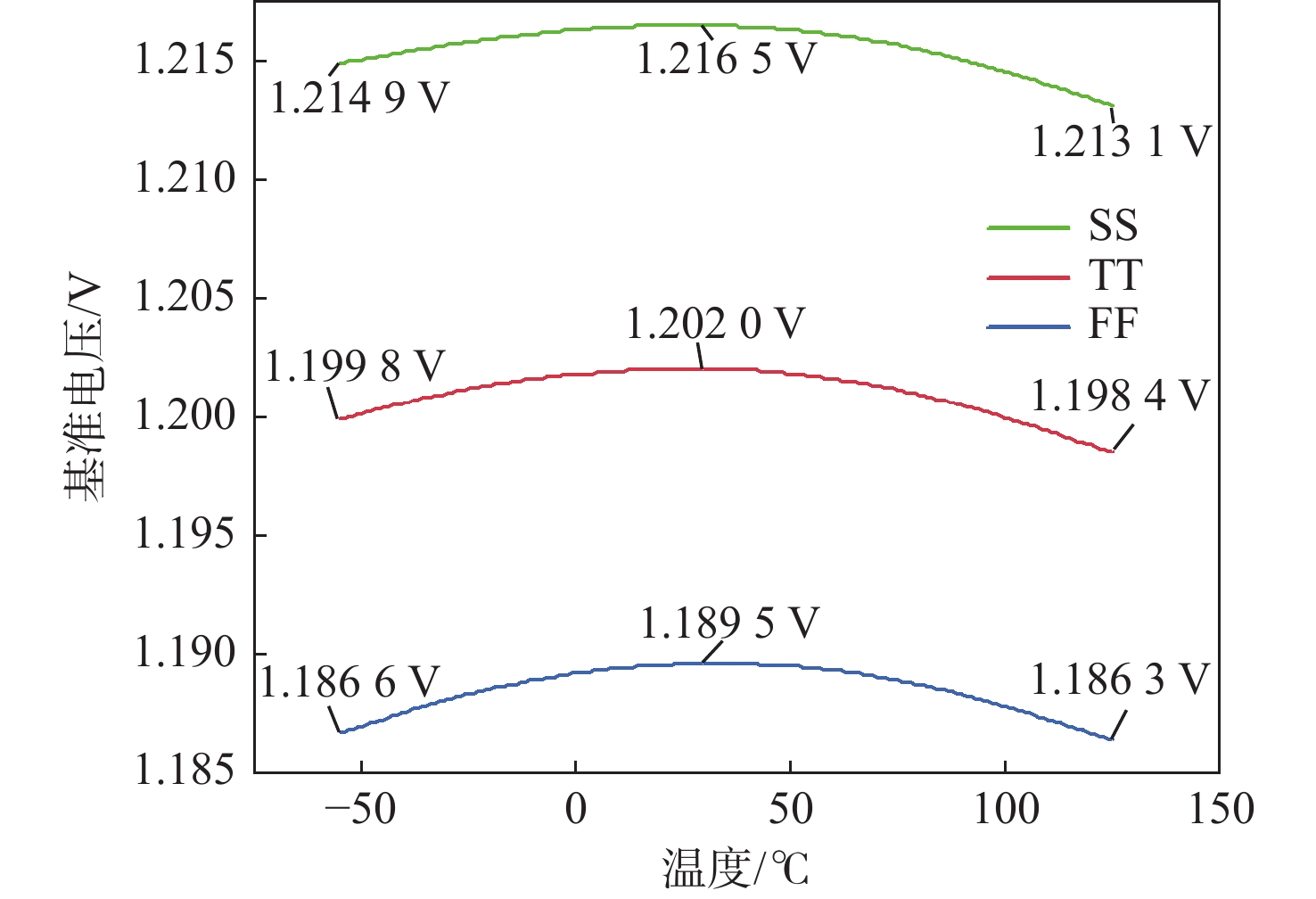
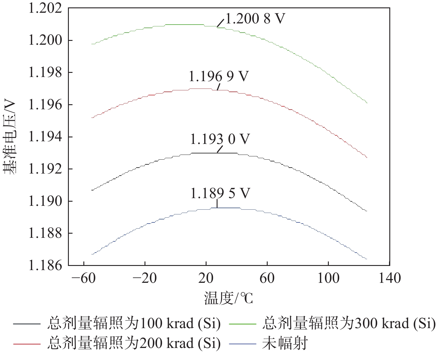
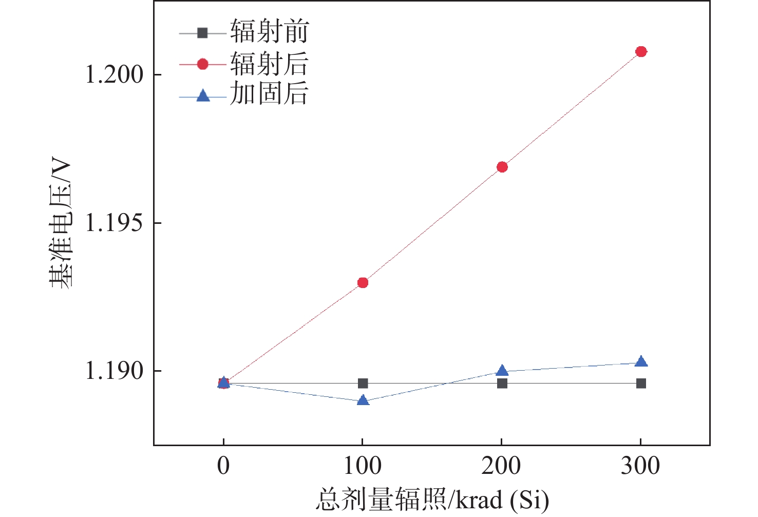
图 7 TT工艺角下,辐照后的带隙基准电压
Figure 7. Bandgap reference voltage after irradiation at TT process angle
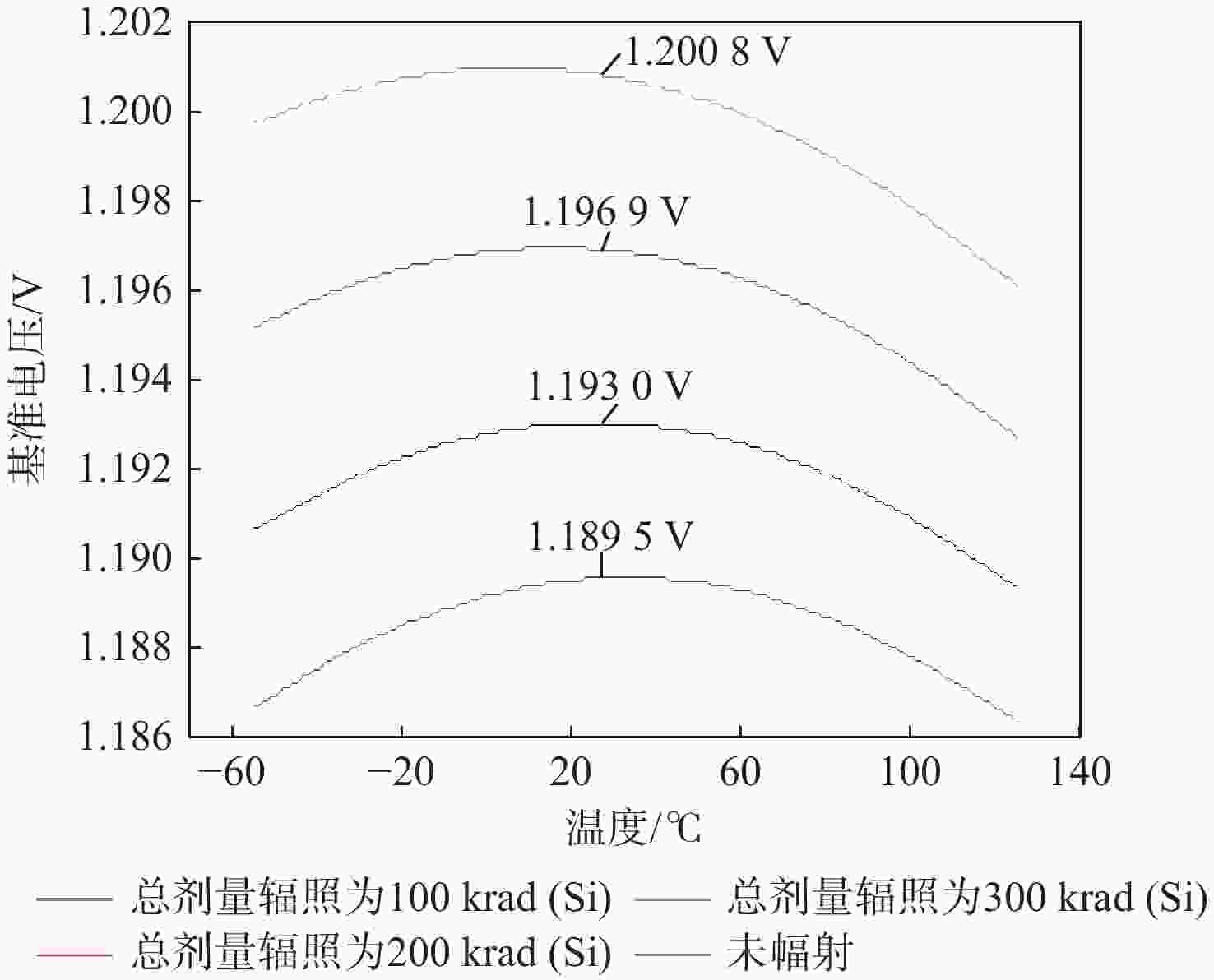
图 8 FF工艺角下,辐照后的带隙基准电压
Figure 8. Bandgap reference voltage after irradiation at FF process angle
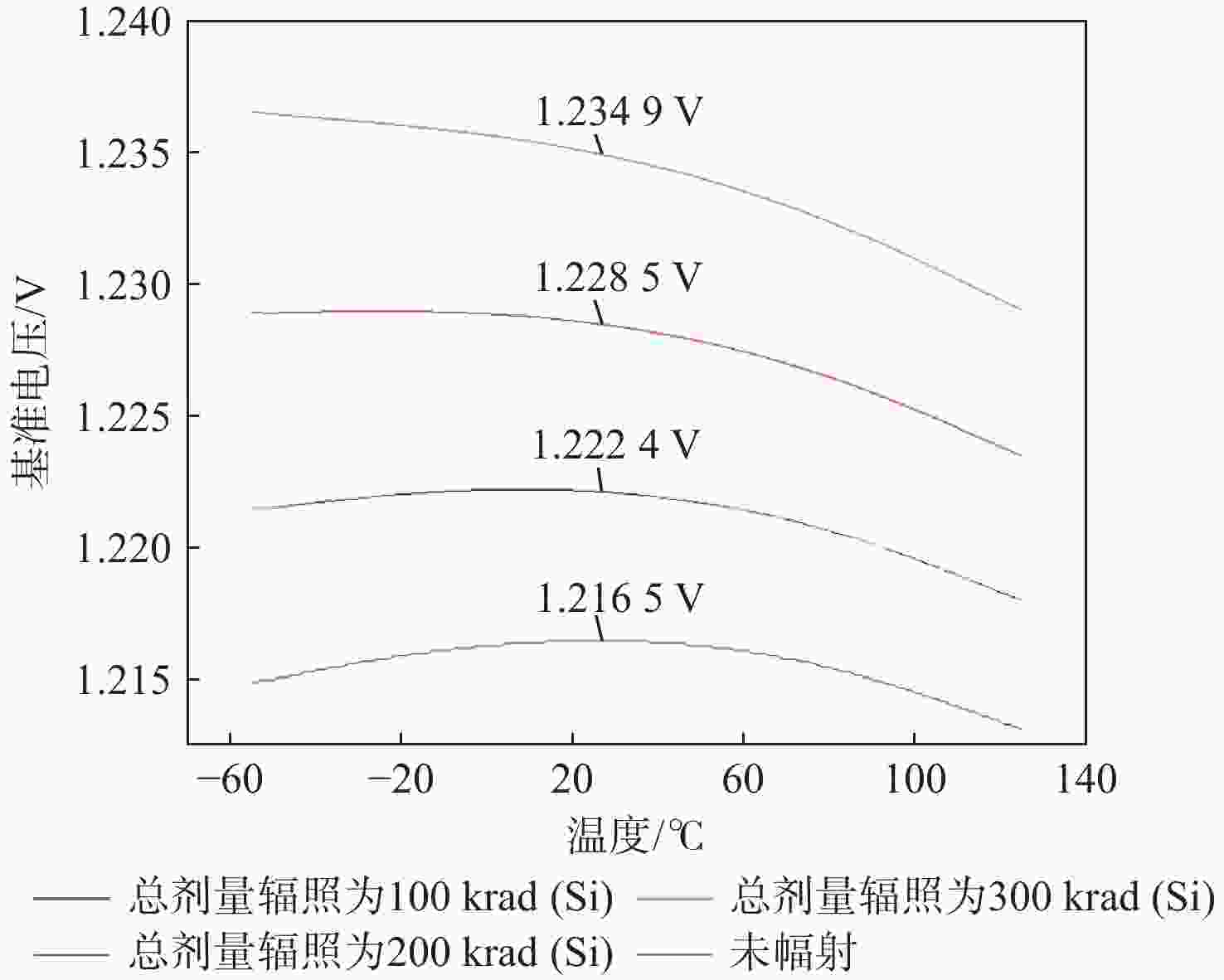
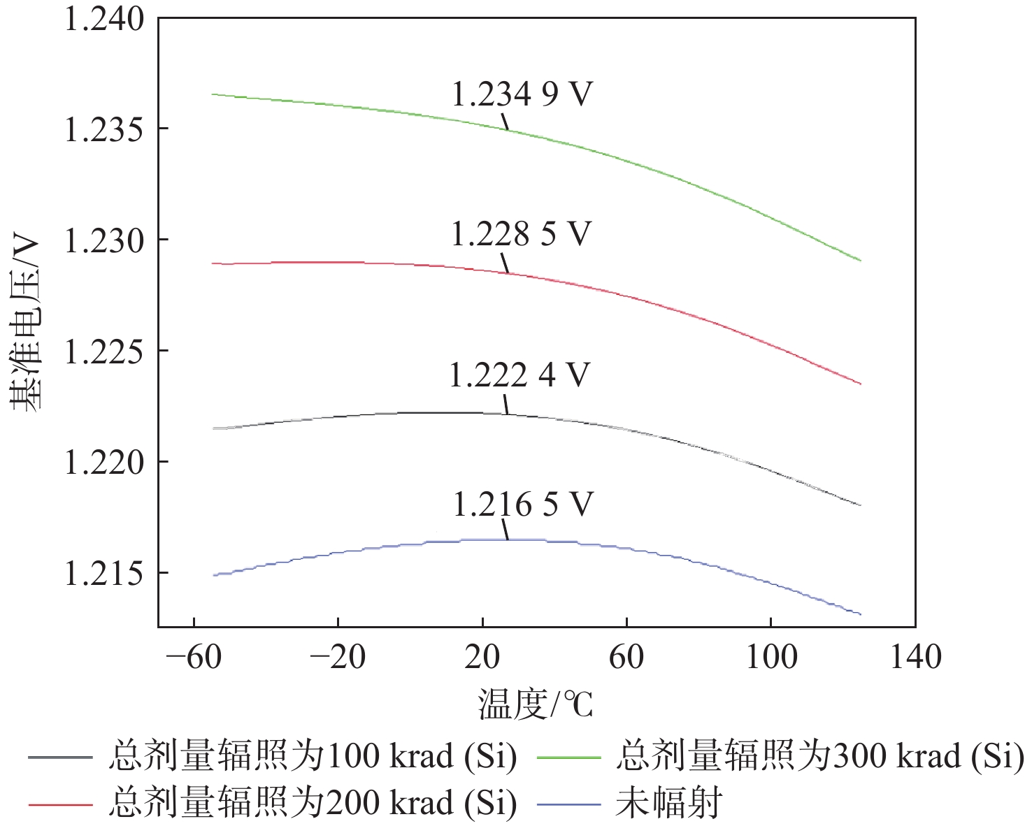
图 9 SS工艺角下,辐照后的带隙基准电压
Figure 9. Bandgap reference voltage after irradiation at SS process angle
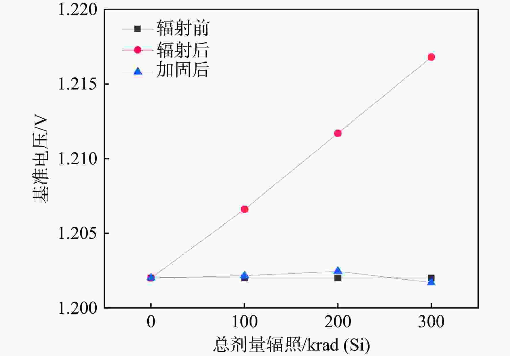
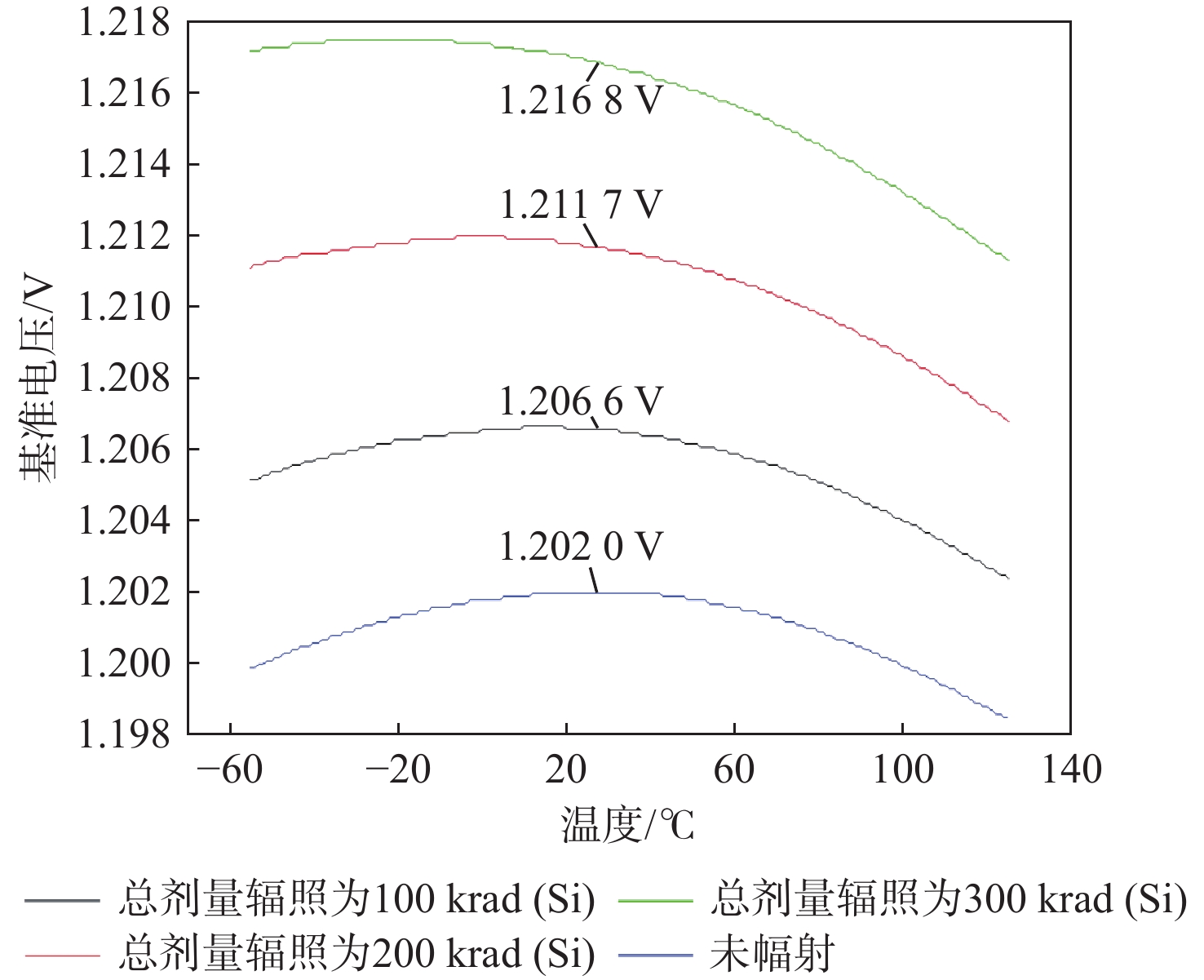
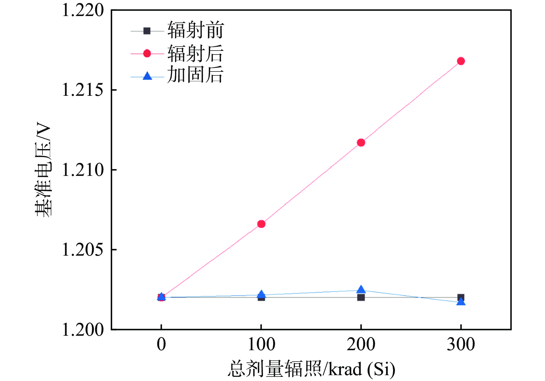
图 10 TT工艺角下,加固后的带隙基准电压
Figure 10. Bandgap reference voltage after reinforcement at TT process angle
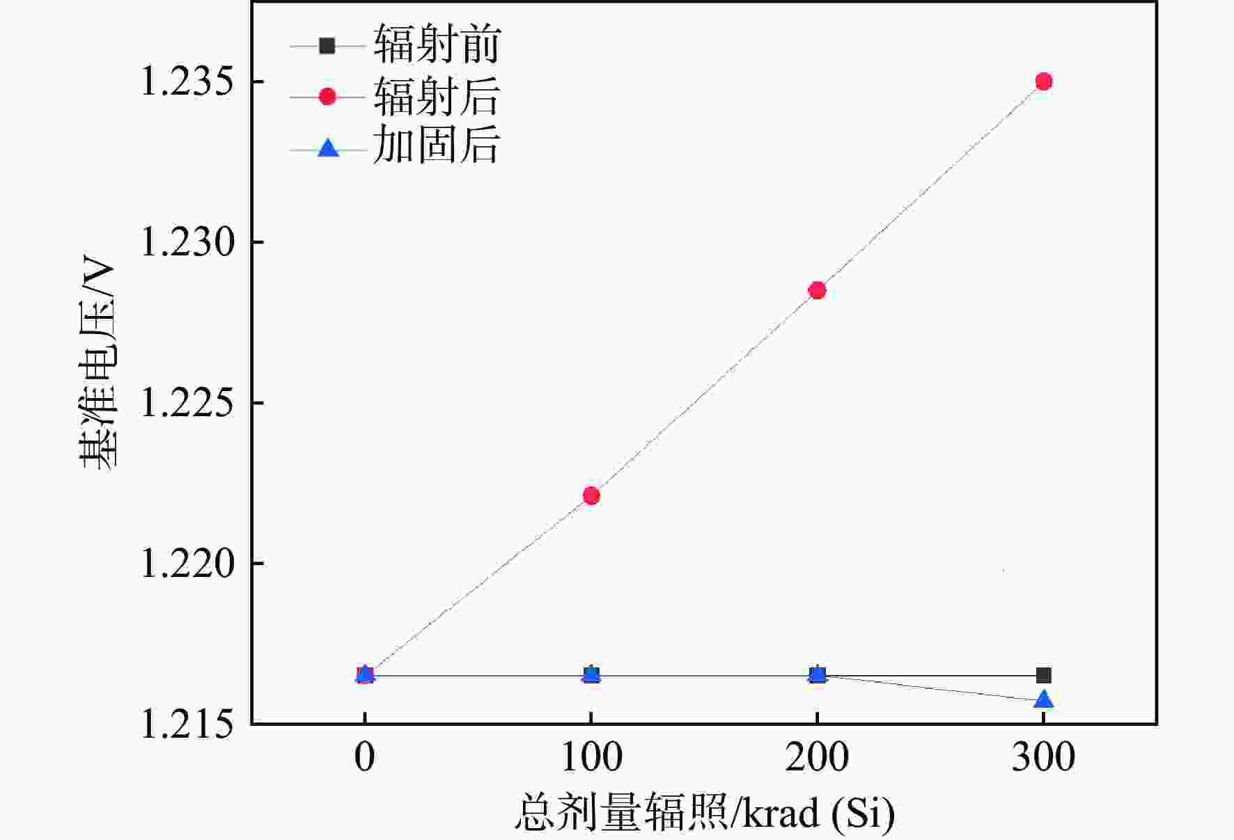
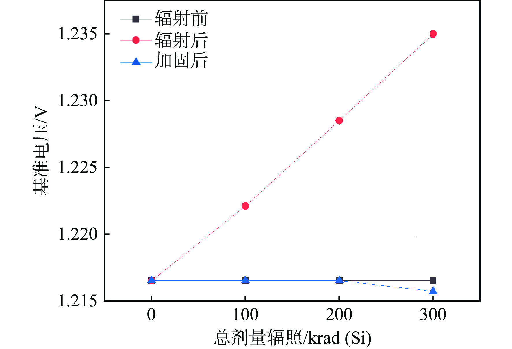
图 11 SS工艺角下,加固后的带隙基准电压
Figure 11. Bandgap reference voltage after reinforcement at SS process angle
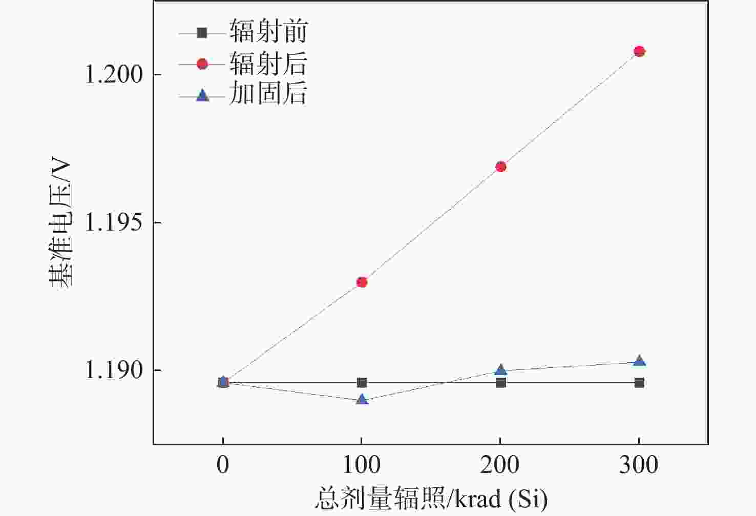
图 12 FF工艺角下,加固后的带隙基准电压
Figure 12. Bandgap reference voltage after reinforcement at FF process angle
表 1 不同工艺角下加固前后对比
Table 1. Comparison of reinforcement before and after different process angles
工艺角 输出电压/V 加固后的输出电压范围/V 辐照前总剂量辐照 总剂量辐照为100 krad(Si) 总剂量辐照为200 krad(Si) 总剂量辐照为300 krad(Si) TT 1.2020 1.2066 1.2117 1.2168 1.20168 ~1.20245 SS 1.2165 1.2224 1.2285 1.2349 1.21570 ~1.21650 FF 1.1895 1.1930 1.1969 1.2008 1.18900 ~1.19030  下载: 导出CSV
-
[1] LI T H, YANG Y T, LIU J, et al. Forward body bias for characterizing TID effect in CMOS integrated circuits[C]//Proceedings of the IEEE 24th International Symposium on the Physical and Failure Analysis of Integrated Circuits. Piscataway: IEEE Press, 2017: 1-5. [2] KUMAR M, UBHI J S, BASRA S, et al. Total ionizing dose hardness analysis of transistors in bias for characterizing TID effect in CMOS integrated circuits[J]. Microelectronics Journal, 2021, 115: 105182. doi: 10.1016/j.mejo.2021.105182 [3] 刘凡. 宇航用抗辐射关键模拟单元电路的研究与应用[D]. 成都: 电子科技大学, 2017.LIU F. Research and application of anti-radiation key analog unit circuit for aerospace[D]. Chengdu: University of Electronic Science and Technology of China, 2017(in Chinese). [4] CHEN Z J, DING D, SHAN Y, et al. Investigation of TID effects on subthreshold bandgap reference circuits fabricated in a SOI process[C]//Proceedings of the International Conference on Radiation Effects of Electronic Devices. Piscataway: IEEE Press, 2018: 1-3. [5] LIU F, YANG F, WANG H, et al. Radiation-hardened CMOS negative voltage reference for aerospace application[J]. IEEE Transactions on Nuclear Science, 2017, 64(9): 2505-2510. doi: 10.1109/TNS.2017.2733738 [6] 梁盛铭, 向飞, 王菡, 等. 一种抗辐射加固带隙基准的设计方法[J]. 现代应用物理, 2023, 14(1): 154-158.LIANG S M, XIANG F, WANG H, et al. A design method of band gap reference for anti-radiation reinforcement[J]. Modern Applied Physics, 2023, 14(1): 154-158(in Chinese). [7] MCCUE B M, BLALOCK B J, BRITTON C L, et al. A wide temperature, radiation tolerant, CMOS-compatible precision voltage reference for extreme radiation environment instrumentation systems[J]. IEEE Transactions on Nuclear Science, 2013, 60(3): 2272-2279. doi: 10.1109/TNS.2013.2257850 [8] VERGINE T, MICHELIS S, DE MATTEIS M, et al. A 65nm CMOS technology radiation-hard bandgap reference circuit[C]//Proceedings of the 10th Conference on Ph. D. Research in Microelectronics and Electronics. Piscataway: IEEE Press, 2014: 1-4. [9] 刘智, 杨力宏, 姚和平, 等. 抗辐射加固CMOS基准设计[J]. 太赫兹科学与电子信息学报, 2017, 15(1): 125.LIU Z, YANG L H, YAO H P, et al. Design of a total-dose radiation hardened CMOS reference[J]. Journal of Terahertz Science and Electronic Information Technology, 2017, 15(1): 125(in Chinese). [10] WU Y C, LUO P, ZHANG B. Neutron and total ionizing dose irradiation hardened LDO[C]//Proceedings of the IEEE 16th International Conference on Solid-State & Integrated Circuit Technology. Piscataway: IEEE Press, 2022: 1-3. [11] SHETLER K J, HOLMAN W T, KAUPPILA J S, et al. Total dose measurement circuit design based on a voltage reference topology[J]. IEEE Transactions on Nuclear Science, 2016, 64(1): 559-566. [12] GROMOV V, ANNEMA A J, KLUIT R, et al. A radiation hard bandgap reference circuit in a standard 0.13 μm CMOS technology[J]. IEEE Transactions on Nuclear Science, 2007, 54(6): 2727-2733. doi: 10.1109/TNS.2007.910170 [13] PRIVAT A, DAVIS P W, BARNABY H J, et al. Total dose effects on negative and positive low-dropout linear regulators[J]. IEEE Transactions on Nuclear Science, 2020, 67(7): 1332-1338. doi: 10.1109/TNS.2020.2977296 [14] 王鹏. 基于标准CMOS工艺的抗辐射带隙基准电路设计[J]. 微处理机, 2016, 37(3): 13-16.WANG P. Design radiation hardened bandgap reference circuit based on standard CMOS technology[J]. Microprocessors, 2016, 37(3): 13-16(in Chinese). [15] FERRARO R, ALÍA R G, DANZECA S, et al. Analysis of bipolar integrated circuit degradation mechanisms against combined TID–DD effects[J]. IEEE Transactions on Nuclear Science, 2021, 68(8): 1585-1593. doi: 10.1109/TNS.2021.3082646 [16] 李顺, 宋宇, 周航, 等. 双极型晶体管总剂量效应的统计特性[J]. 物理学报, 2021, 70(13): 363-368.LI S, SONG Y, ZHOU H, et al. Statistical characteristics of total ionizing dose effects of bipolar transistors[J]. Acta Physica Sinica, 2021, 70(13): 363-368(in Chinese). [17] ADAMS D A, BARNES H A, GOLDSTEIN N P, et al. A total ionizing dose dataset for vertical NPN transistors[C]//Proceedings of the IEEE Radiation Effects Data Workshop. Piscataway: IEEE Press, 2014: 1-3. [18] PRIVAT A, BARNABY H J, TOLLESON B S, et al. Temperature response on NPN and PNP bipolar junction transistors after total ionizing dose irradiation exposure[C]//Proceedings of the 19th European Conference on Radiation and Its Effects on Components and Systems. Piscataway: IEEE Press, 2019: 1-6. [19] ZEBREV G I, PETROV A S , USEINOV R G , et al. Simulation of bipolar transistor degradation at various dose rates and electrical modes for high dose conditions[J]. IEEE Transactions on Nuclear Science, 2009, 61(4): 2505-2510. [20] ZHANG T, LIU Y, EN Y F, et al. Experiment and numerical simulation of total dose effects in the substrate PNP transistors[C]//Proceedings of the International Conference on Quality, Reliability, Risk, Maintenance, and Safety Engineering. Piscataway: IEEE Press, 2013: 1030-1032. -

 下载:
下载:

 点击查看大图
计量
- 文章访问数: 232
- HTML全文浏览量: 138
- PDF下载量: 7
- 被引次数: 0
