


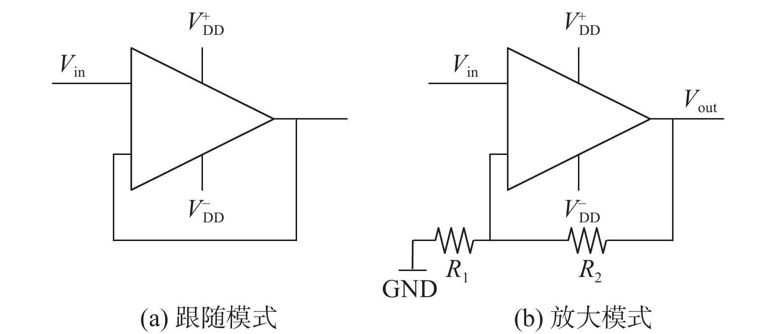
Mechanism of anomalies in operational amplifier induced by proton deep charge-discharge effects
-
摘要:
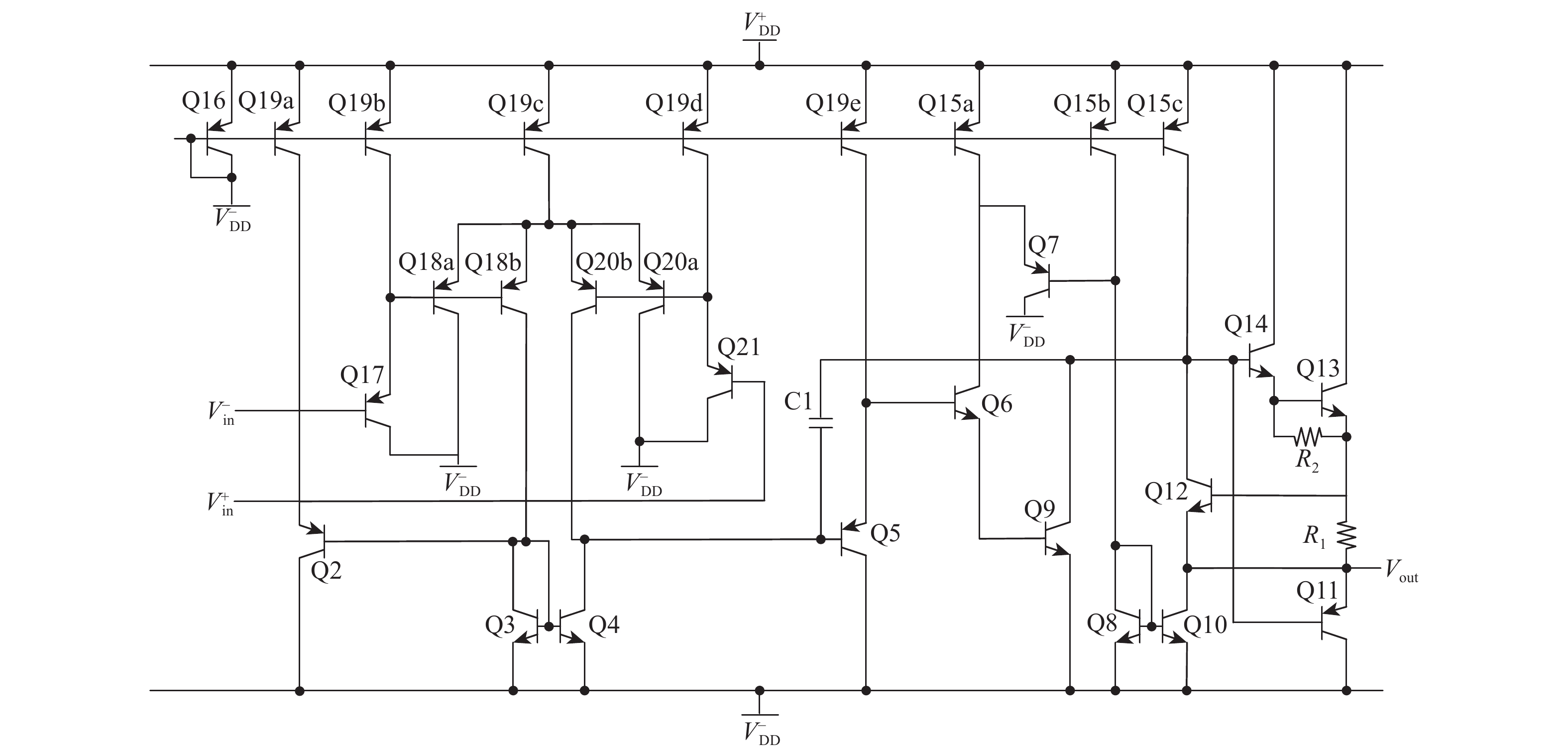
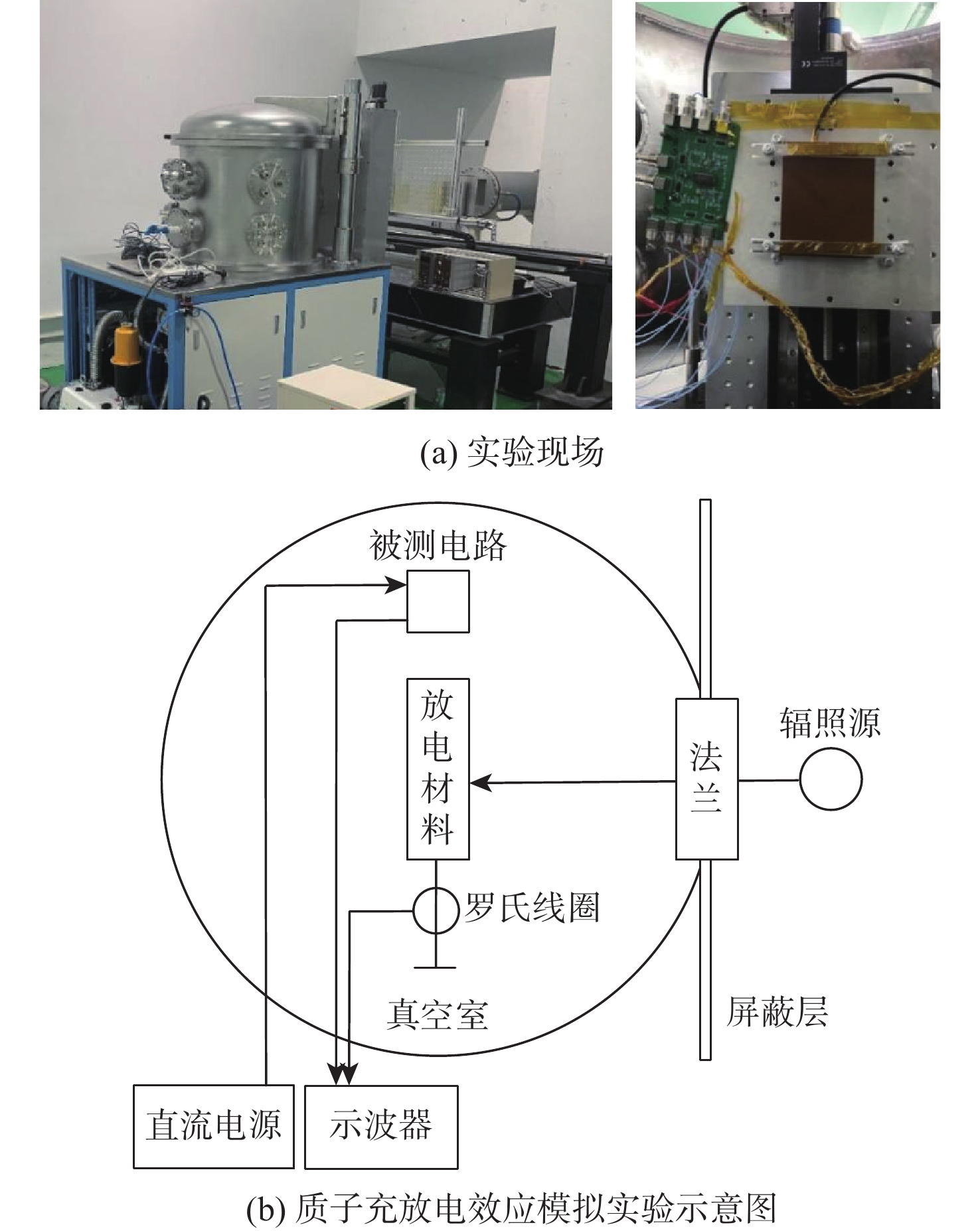
中高能太阳质子和银河宇宙线作为在深空轨道运行的航天器主要遭遇的辐射环境,大量入射至电介质材料将诱发深层充放电效应,导致电子器件工作状态异常。以LM124运算放大电路为研究示例,使用中高能质子加速器研究深空质子致深层充放电效应诱发电路产生异常的特征规律,同时结合H-集成电路性能分析电路仿真程序(HSPICE)仿真研究运算放大电路的深层充放电效应敏感区域与机理。结果表明:质子深层充电诱发的航天器静电放电(SESD)将导致运算放大电路输出异常瞬态,输出瞬态的幅值与SESD脉冲的幅值正相关,瞬态的持续时间与电路工作状态有关;电路的负电源输入端是SESD的敏感区域;输入控制晶体管与增益晶体管受SESD影响输出电流瞬态并导致电路输出异常是主要的故障机理。
Abstract:When solar protons and galactic cosmic rays, the primary radiation environments in deep space, accumulate in the dielectric material, they can cause spacecraft electrostatic discharge induced by charging (SESD), which can cause abnormalities in electronic devices. The LM124 integrated operational amplifier are used to study the characteristics of anomalies. The H-simulation program with integrated circuit enphasis (HSPICE) simulation is used to study the SESD sensitive region and mechanism of anomalies. The findings suggest that the output pin may experience transients due to the SESD transient. The amplitude of the output transient is positively associated with the amplitude of the SESD transient, and the duration of the output transient is associated with the circuit operating state. The negative power pin is the SESD sensitive region. The current transient in the input-control transistors and gain transistors caused by SESD induces output voltage anomalies.
-
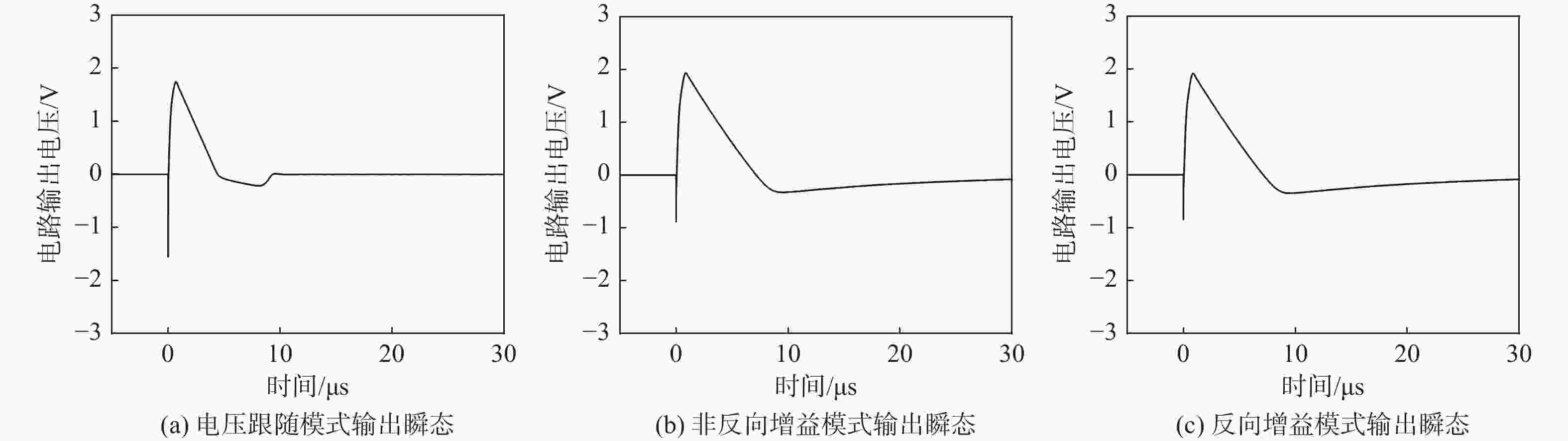
图 6 全管脚注入模式SESD诱发电路输出瞬态
Figure 6. Circuit output transients with SESD all pin injection mode
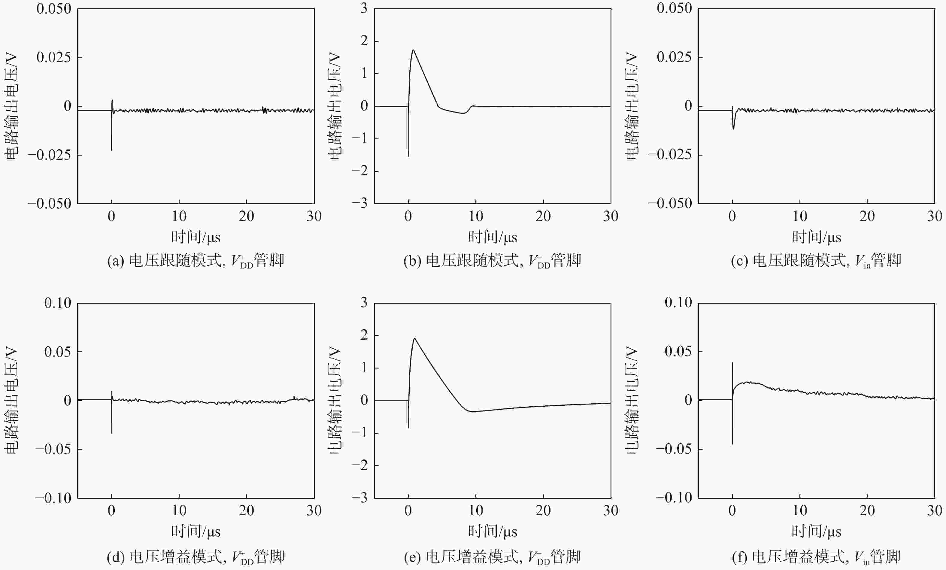
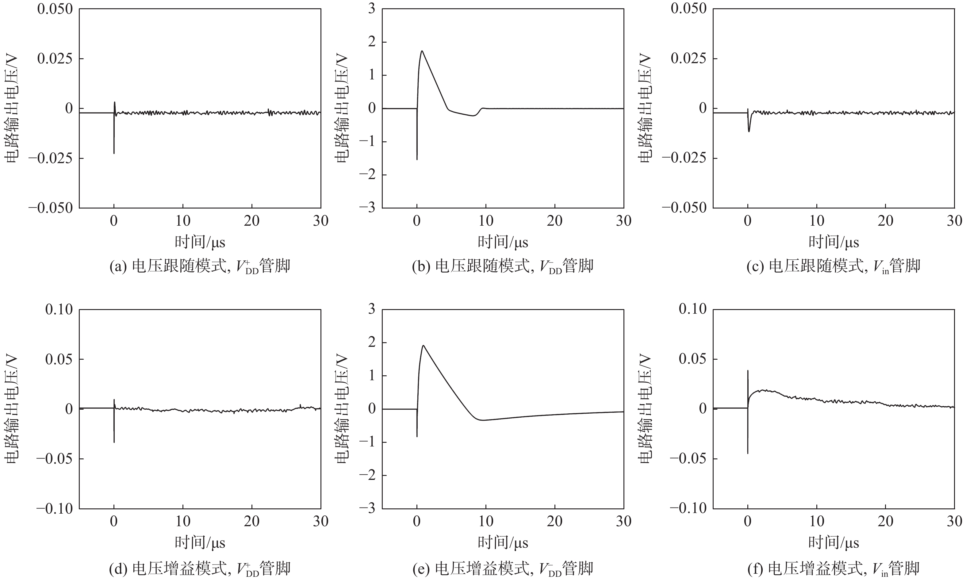
图 7 单管脚注入模式SESD诱发电路输出瞬态
Figure 7. Circuit output transients with SESD single pin injection mode
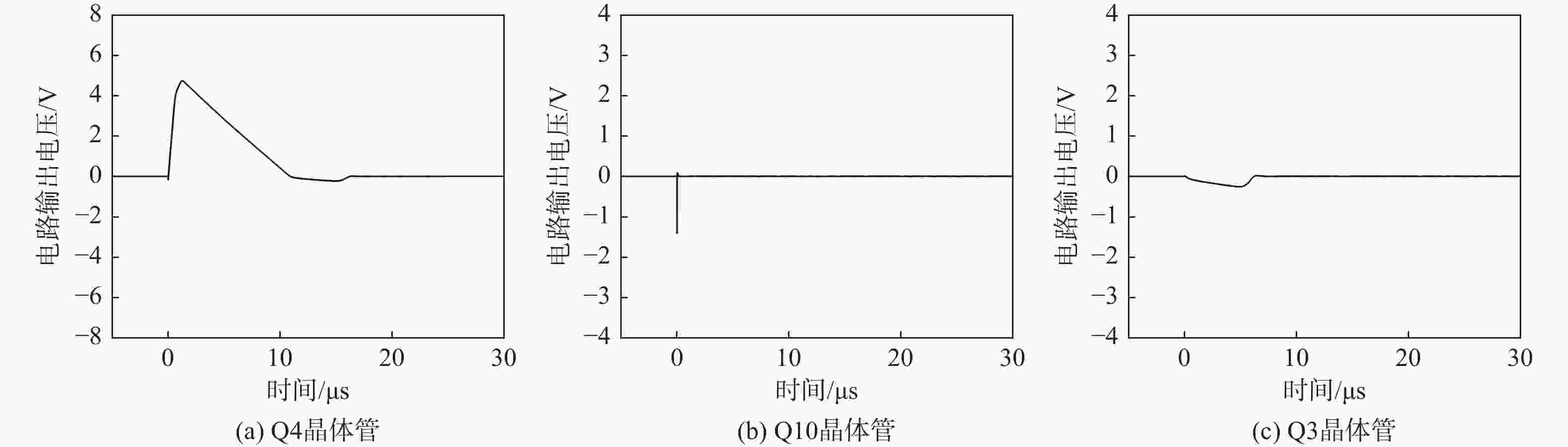
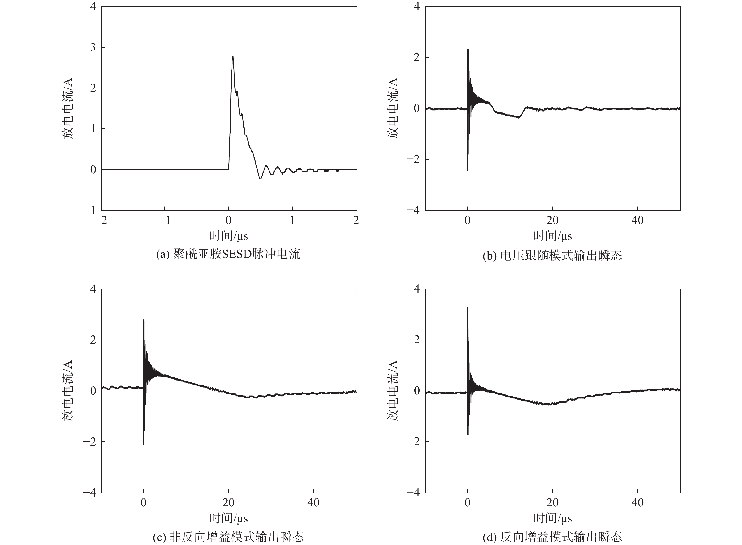
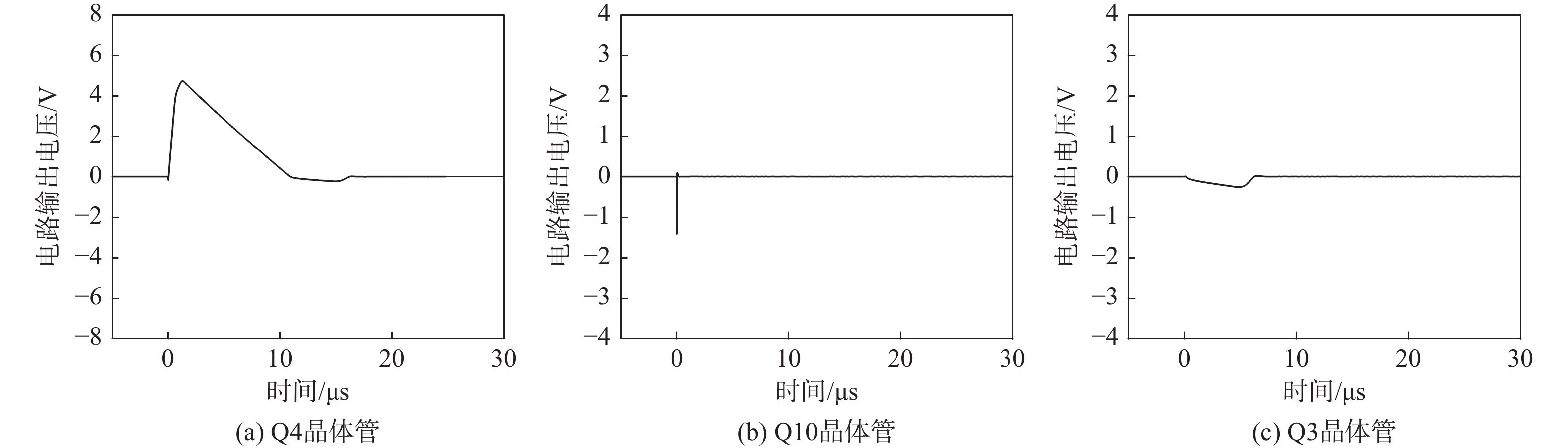
图 8 SESD脉冲注入晶体管诱发电压跟随模式输出瞬态特征
Figure 8. Characteristics of output voltage in transistor caused by SESD transient with voltage following mode

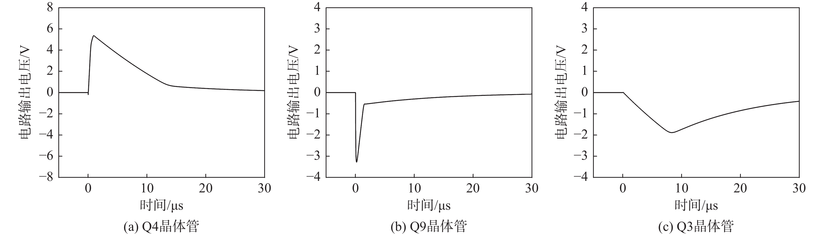
图 9 SESD脉冲注入晶体管诱发电路增益模式输出瞬态特征
Figure 9. Characteristics of output voltage in transistor caused by SESD transient with voltage gain mode
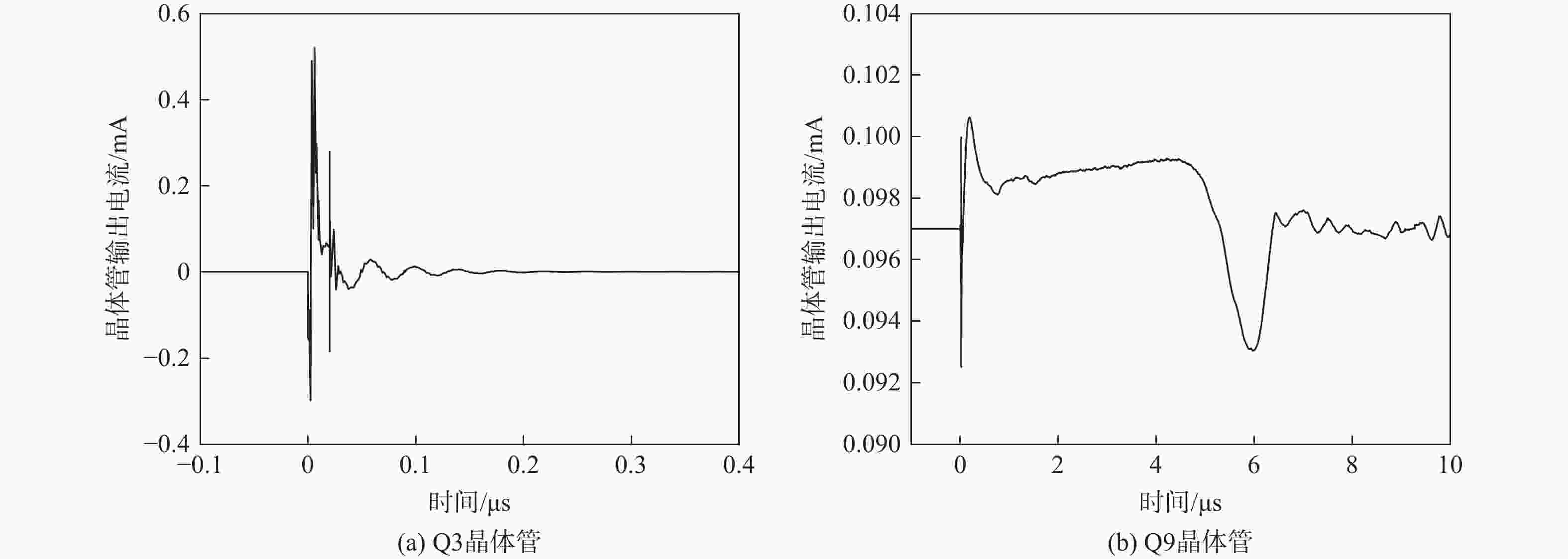
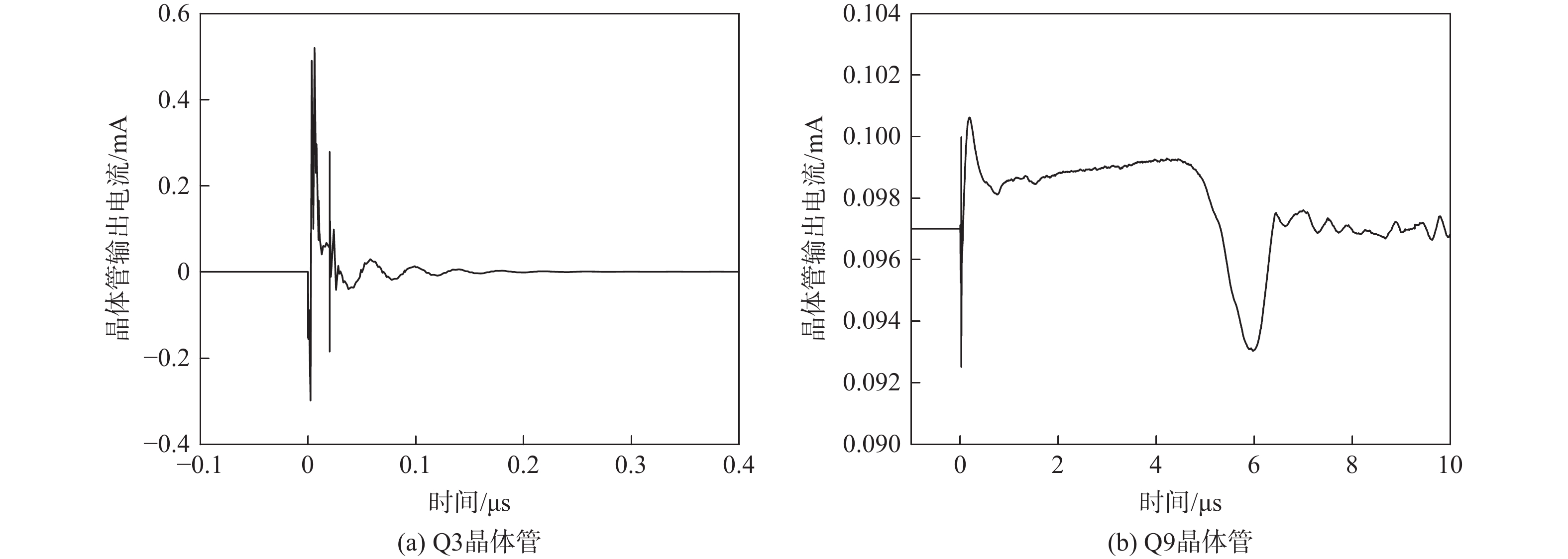
图 10 SESD脉冲注入输入控制晶体管Q3发射极诱发Q3与Q9产生的电流瞬态
Figure 10. Current transients in Q3 and Q9 induced by SESD transient injected into source of Q3
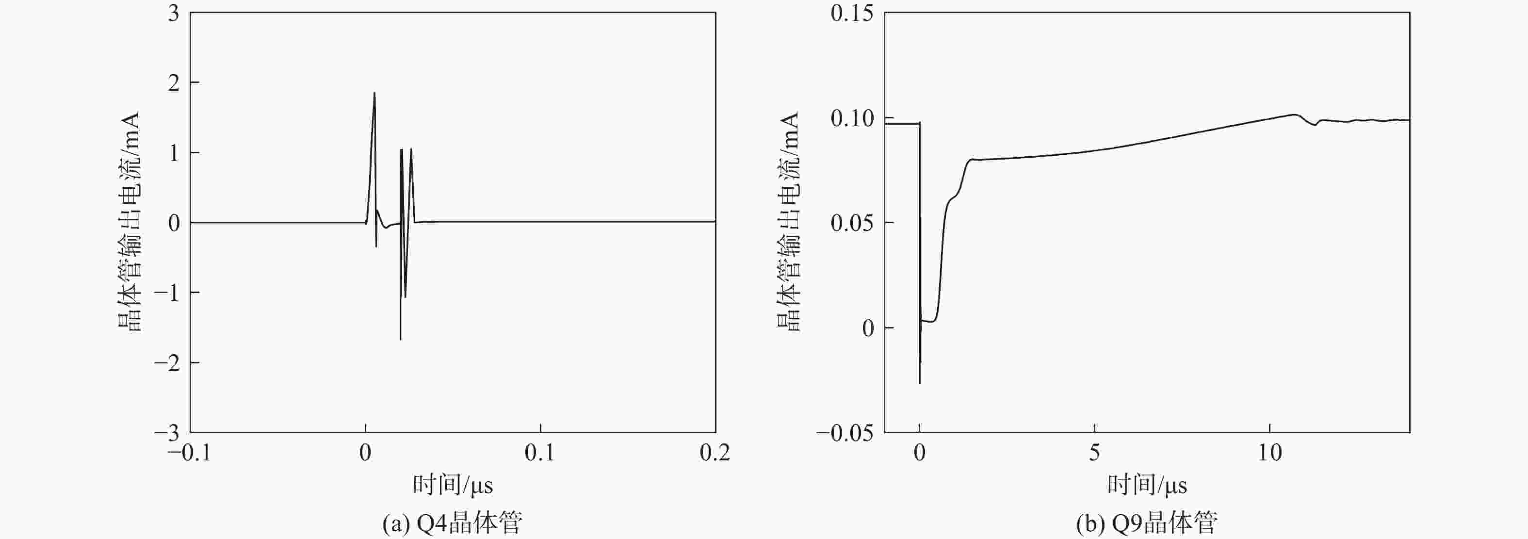
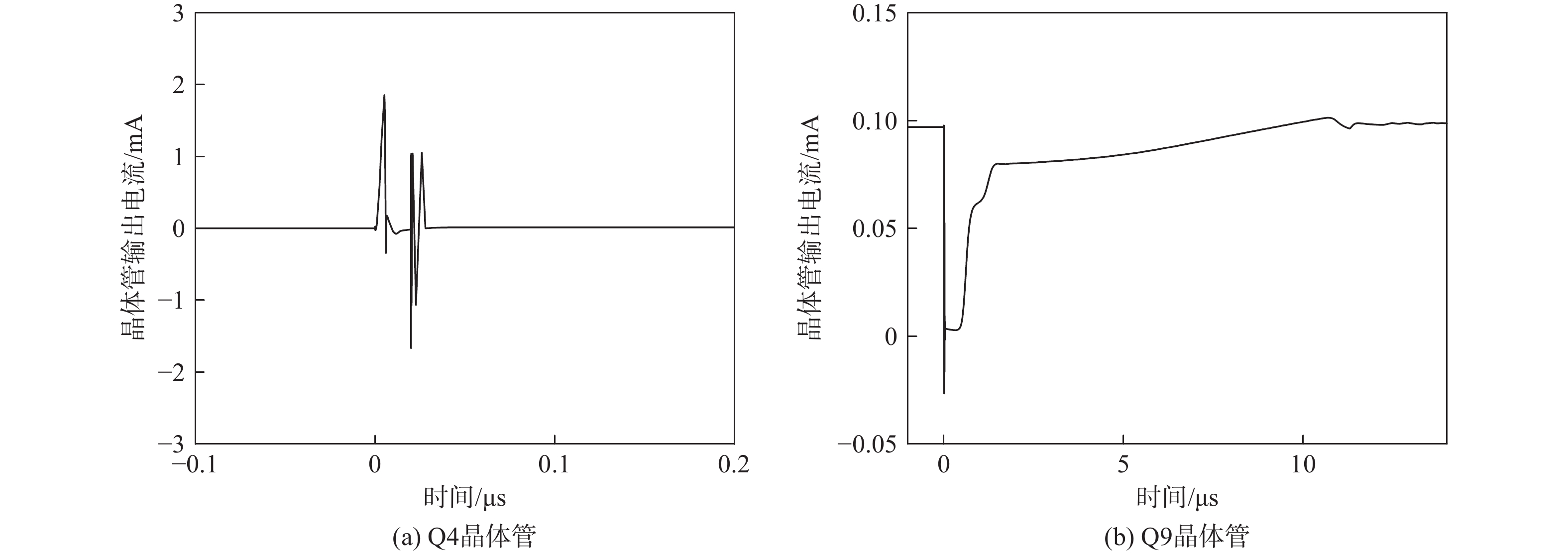
图 11 SESD脉冲注入输入控制晶体管Q4发射极诱发Q4与Q9产生的电流瞬态
Figure 11. Current transients in Q4 and Q9 induced by SESD transient injected into source of Q4

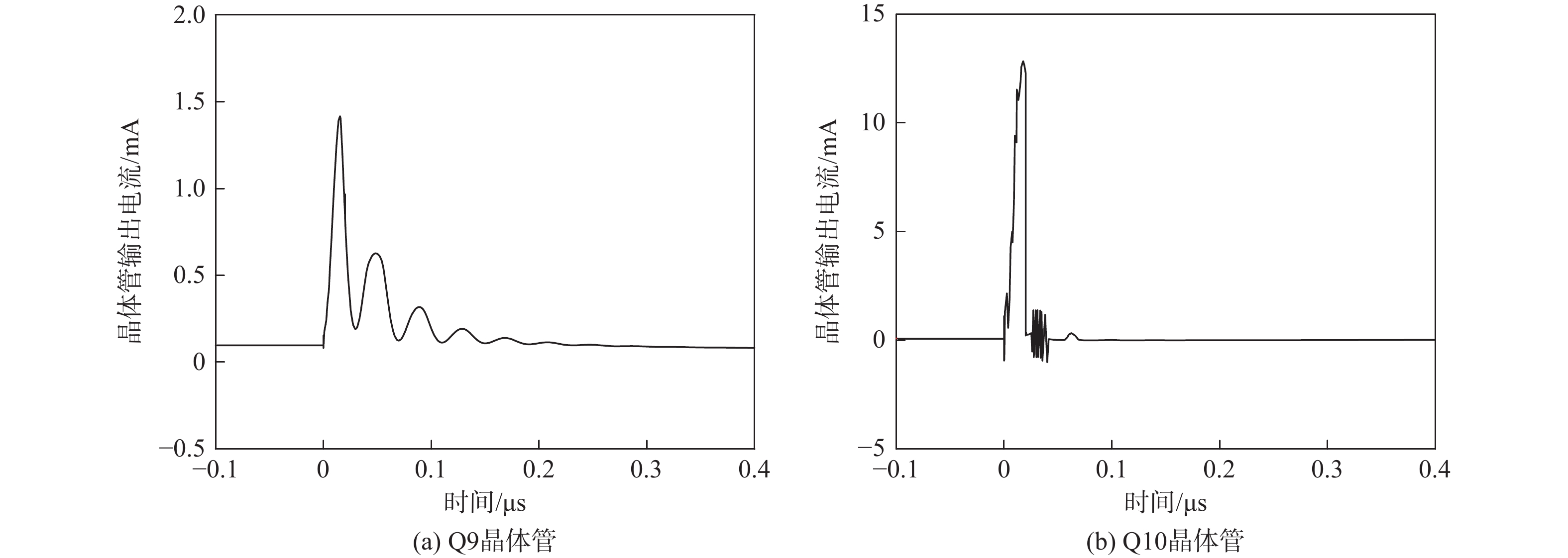
图 12 SESD脉冲注入增益晶体管Q9与偏置晶体管Q10发射极对其发射-集电电流的影响
Figure 12. Current transients in Q9 and Q10 induced by SESD transient injected into source of Q9 and Q10
表 1 运算放大电路输出瞬态特征
Table 1. Transient characteristics of operational amplifier circuit outputs
放电材料
厚度/mm振幅/V 持续时间/μs 电压跟随 非反向增益 反向增益 电压跟随 非反向增益 反向增益 15.5 7.1 7.3 7.4 13.8 24.1 18.7 21.5 2.9 2.8 3.2 14.9 21.2 26.5  下载: 导出CSV
表 2 运算放大电路SESD敏感区域
Table 2. SESD sensitive regions of operational amplifier circuits
SESD脉冲
注入位置振幅/V 持续时间/μs 电压跟随模式 增益模式 电压跟随模式 增益模式 $V_{\mathrm{DD}}^+ $ 0.03 0.04 0.21 0.23 $V_{\mathrm{DD}}^- $ 3.28 2.75 10.18 25.00 $V_{\mathrm{in}} $ 0.01 0.08 0.79 0.01
下载: 导出CSV
-
[1] LEACH R. Spacecraft system failures and anomalies attributed to the natural space environment[C]//Proceedings of the Space Programs and Technologies Conference. Reston: AIAA, 1995. [2] KOONS H C, MAZUR J E, SELESNICK R S, et al. The impact of the space environment on space systems[C]//Proceedings of the 6th Spacecraft Charging Conference. Washington, D. C. : NASA, 2000. [3] ECOFFET R. Overview of in-orbit radiation induced spacecraft anomalies[J]. IEEE Transactions on Nuclear Science, 2013, 60(3): 1791-1815. [4] BAKER D N. The occurrence of operational anomalies in spacecraft and their relationship to space weather[J]. IEEE Transactions on Plasma Science, 2000, 28(6): 2007-2016. [5] VAMPOLA A L. The hazardous space particle environment[J]. IEEE Transactions on Plasma Science, 2000, 28(6): 1831-1839. [6] NUMATA S, MIYAKE H, TANAKA Y, et al. Dielectric characteristic evaluation of proton beam irradiated polyimide films[C]//Proceedings of the Annual Report Conference on Electrical Insulation and Dielectic Phenomena. Piscataway: IEEE Press, 2010: 1-4. [7] RYDEN K A, MORRIS P A, RODGERS D J, et al. Improved demonstration of internal charging hazards using the realistic electron environment facility(REFF)[C]//Proceedings of the 9th Spacecraft Charging Technology Conference. Tokyo: Japan Aerospace Exploration Agency, 2005. [8] FENG W Q, DING Y G, DEKUIWANG Y. Laboratory simulation of spacecraft surface charging and discharging caused structural potential transients and its interference test method on DC-DC converter[C]//Proceedings of the Spacecraft Charging Technology Conference. Washington, D. C.: NASA, 2001. [9] 冯伟泉, 王志浩, 万成安, 等. GEO卫星表面充放电引起卫星地电位瞬变及对二次电源干扰试验研究[J]. 航天器环境工程, 2013, 30(1): 54-57.FENG W Q, WANG Z H, WAN C A, et al. GEO satellite ground potential transients caused by surface charging & discharging and their interferences on secondary power supply[J]. Spacecraft Environment Engineering, 2013, 30(1): 54-57(in Chinese). [10] WANG J L, ZHANG Z L. The ground simulation of spacecraft discharge impacts on the space environment detectors[J]. IEEE Transactions on Plasma Science, 2016, 44(7): 1247-1253. [11] 张振龙, 韩建伟, 全荣辉, 等. 空间材料深层充放电效应试验研究[J]. 航天器环境工程, 2009, 26(3): 210-213.ZHANG Z L, HAN J W, QUAN R H, et al. Experiment on deep dielectric charging and discharging of space materials[J]. Spacecraft Environment Engineering, 2009, 26(3): 210-213(in Chinese). [12] CHEN R, CHEN L, LI S, et al. Comparative study on the transients induced by single event effect and space electrostatic discharge[J]. IEEE Transactions on Device and Materials Reliability, 2019, 19(4): 733-740. [13] 郑汉生, 朱翔, 陈睿, 等. 空间静电放电对集成运算放大器的干扰影响模拟试验研究[J]. 中国科学: 技术科学, 2017, 47(1): 80-88.ZHENG H S, ZHU X, CHEN R, et al. Simulated experiment research on SESD interference with integrated operational amplifier[J]. Scientia Sinica (Technologica), 2017, 47(1): 80-88(in Chinese). [14] WANG X, CHEN R, YUAN R J, et al. Experimental study on the space electrostatic discharge effect and the single event effect of SRAM devices for satellites[J]. Applied Sciences, 2022, 12(14): 7129. [15] WANG X, CHEN R, HAN J W, et al. Comparative experimental study on space electrostatic discharge effect and single event effect of 130 nm SOI D flip-flop chains[J]. Atomic Energy Science and Technology, 2021, 55(12): 2191-2200. [16] GREEN N W, DENNISON J R. Deep dielectric charging of spacecraft polymers by energetic protons[J]. IEEE Transactions on Plasma Science, 2008, 36(5): 2482-2490. [17] 秦晓刚, 贺德衍, 杨生胜, 等. 行星际空间质子引起介质深层充电的GEANT4模拟研究[J]. 宇航学报, 2010, 31(2): 526-530.QIN X G, HE D Y, YANG S S, et al. Geant4 simulation of interplanetary proton induced deep dielectrics charging[J]. Journal of Astronautics, 2010, 31(2): 526-530(in Chinese). [18] 齐晓华. 基础物理实验中RC微积分电路的Multisim仿真[J]. 电子设计工程, 2012, 20(3): 37-38.QI X H. Multisim simulation on RC calculus circuit in fundamental physics experiments[J]. Electronic Design Engineering, 2012, 20(3): 37-38(in Chinese). [19] BOULGHASSOUL Y, MASSENGILL L W, STERNBERG A L, et al. Circuit modeling of the LM124 operational amplifier for analog single-event transient analysis[J]. IEEE Transactions on Nuclear Science, 2002, 49(6): 3090-3096. [20] CHEN R, HAN J W, ZHENG H S, et al. Comparative research on “high currents” induced by single event latch-up and transient-induced latch-up[J]. Chinese Physics B, 2015, 24(4): 046103. [21] KER M D, HSU S F. Component-level measurement for transient-induced latch-up in CMOS ICs under system-level ESD considerations[J]. IEEE Transactions on Device and Materials Reliability, 2006, 6(3): 461-472. [22] KER M D, HSU K C. Native-NMOS-triggered SCR with faster turn-on speed for effective ESD protection in a 0.13-$rm murm m$CMOS process[J]. IEEE Transactions on Device and Materials Reliability, 2005, 5(3): 543-554. -

 下载:
下载:


 点击查看大图
计量
- 文章访问数: 306
- HTML全文浏览量: 103
- PDF下载量: 20
- 被引次数: 0
