


-
摘要:
研究了三维集成电路(3D ICs)中硅通孔(TSV)的建模方法及三维集成电路电源分配网络(PDN)的建模方法,并结合印制电路板(PCB)的电源分布网络和芯片PDN模型,提出了一种对板级三维集成电路进行电源网络上电磁敏感性(EMS)的建模和协同分析方法。首先给出了地-信号(GS)结构和地-信号1-信号2-地(GSSG)结构TSV的电路模型,电路模型与数值仿真结果做了对比,验证了TSV电路建模方法的准确性。接着对PCB板级三维集成电路中PCB的电源分布网络,PCB过孔,集成电路封装参数进行建模。最后创建了一个PCB-三维集成电路电磁敏感性级联分析模型,使用该模型来研究三维集成电路对电源干扰的敏感特性,并由此指导三维集成电路的敏感性分析。
-
关键词:
- 硅通孔(TSV) /
- TSV电路模型 /
- 电源分配网络(PDN) /
- 电磁敏感性(EMS) /
- 印制电路板(PCB)
Abstract:This paper focuses on the circuit modeling method of through silicon via (TSV) and power distribution network (PDN) in 3D integrated circuits (3D ICs). Combined with the PDN on printed circuit board (PCB) and the chip PDN model, an electromagnetic susceptibility (EMS) modeling and collaborative analysis method for 3D ICs on PCB was proposed. Firstly, a ground-signal (GS) TSV pair and two TSV pairs of ground-signal1-signal2-ground (GSSG) were established in, and these circuit models were compared with the numerical simulation results, which validated the accuracy of the circuit modeling method of TSV. Then, the modeling method of PDN of PCB, PCB through via hole, IC's package parameters in an IC were discussed. Finally, an EMS cascade connection analysis model from PCB to 3D ICs was developed and used to analyze the electromagnetic susceptibility characteristics of 3D ICs to power interference, which can guide the susceptibility analysis of 3D ICs.
-

图 3 HFSS和ADS中S11和S21的结果对比
Figure 3. Comparison of S11 and S21 resultsbetween HFSS and ADS

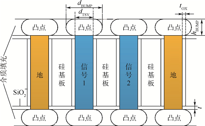
图 4 GSSG结构的TSV示意图
dBUMP—凸点直径;dTSV—TSV直径;hBUMP—凸点高度。
Figure 4. Schematic diagram of GSSG-structure TSV

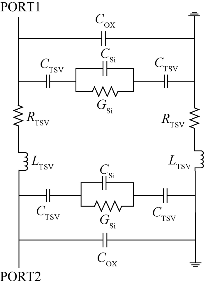
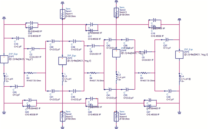
图 6 ADS中建立的GSSG结构TSV的等效电路图
Figure 6. Equivalent circuit diagram of GSSG-structure TSV in ADS

图 7 HFSS和ADS中S参数仿真结果对比
Figure 7. Comparison of S parameter simulation results between HFSS and ADS

图 9 单个过孔结构的分解示意图
Figure 9. Schematic diagram of single via hole structure divided into small parts

图 13 在电源过孔中心电源/地平面间设置集总端口
Figure 13. Lumped port added between power and ground plane in center of power via hole
表 1 GS结构TSV对的模型参数
Table 1. Model parameters of GS-structure TSV pair
μm 参数 数值 h 100 rTSV 10 tOX 0.6 pTSV 40 t 1 t1 1 注:tOX—SiO2厚度;t1—铜平面厚度;t—SiO2平面厚度。  下载: 导出CSV
表 2 GSSG结构TSV的模型参数
Table 2. Model parameters of GSSG-structure TSV
μm 参数 数值 hTSV 100 rTSV 10 tOX 0.6 pTSV 40 rBUMP 15 hBUMP 5 t 1 注:rBUMP—凸点半径; hTSV—TSV高度。
下载: 导出CSV
表 3 GSSG结构TSV的材料特性
Table 3. Material characteristics of GSSG-structure TSV
参数 数值 σSi/(S·m-1) 10 σTSV/(107 S·m-1) 5.8 σBUMP/(107 S·m-1) 5.8 εr, Si 11.9 εr, OX 4 εr, BCB 2.65 μr, TSV 1 μr, BUMP 1 注:σBUMP—凸点电导率;εr, Si—硅相对介电常数;εr, BCB —BCB相对介电常数;μr, TSV、μr, BUMP —TSV、凸点相对磁导率。
下载: 导出CSV
表 4 BGA封装的pin1~pin4的参数提取结果
Table 4. Parameter extraction results of BGA package from pin1 to pin4
电阻/Ω 电容与互容/pF 自感与互感/nH R11=0.143 C11=0.209 L11=3.732 R22=0.142 C22=0.221 L22=3.697 R33=0.134 C33=0.218 L33=3.408 R44=0.122 C44=0.210 L44=3.092 C12=0.073 L21=1.621 C23=0.071 L13=1.062 C24=0.002 L14=0.521 C34=0.060 L23=1.492 C13=0.002 L24=0.619 L34=0.749
下载: 导出CSV
-
[1] KNICKERBOCKER J U, ANDRY P S, DANG B, et al.3D silicon integration[C]//200858th Electronic Components and Technology Conference.Piscataway, NJ:IEEE Press, 2008:538-543. [2] CADIX L, FARCY A, BERMOND C, et al.Modelling of through silicon via RF performance and impact on signal transmission in 3D integrated circuits[C]//IEEE International Conference on 3D System Integration, 2009.Piscataway, NJ:IEEE Press, 2009:1-7. http://ieeexplore.ieee.org/xpl/articleDetails.jsp?reload=true&tp=&arnumber=5306592&openedRefinements%3D*%26rowsPerPage%3D100%26queryText%3D%283d+circuits+%29 [3] ZHU Y, MA S, SUN X, et al.Developssment and characterization of a through-multilayer TSV integrated SRAM module[C]//2013 IEEE 63rd Electronic Components and Technology Conference.Piscataway, NJ:IEEE Press, 2013:885-890. http://ieeexplore.ieee.org/document/6575678/ [4] KIM J S, OH C S, LEE H, et al.A 1.2V 12.8GB/s 2Gb mobile Wide-I/O DRAM with 4×128 I/Os using TSV-based stacking[C]//2011 IEEE International Solid-State Circuits Conference.Piscataway, NJ:IEEE Press, 2011:496-498. [5] YOON K, KIM G, LEE W, et al.Modeling and analysis of coupling between TSVs, metal, and RDL interconnects in TSV-based 3D IC with silicon interposer[C]//Electronics Packaging Technology Conference, 2009.Piscataway, NJ:IEEE Press, 2009:702-706. [6] HAN K J, SWAMINATHAN M, JEONG J.Modeling of through-silicon via (TSV) interposer considering depletion capacitance and substrate layer thickness effects[J].IEEE Transactions on Components, Packaging and Manufacturing Technology, 2015, 5(1):108-118. doi: 10.1109/TCPMT.2014.2372771 [7] NDIP I, ZOSCHKE K, LBICKE K, et al.Analytical, numerical-, and measurement-based nethods for extracting the electrical parameters of through silicon vias (TSVs)[J].IEEE Transactions on Components, Packaging and Manufacturing Technology, 2014, 4(3):504-515. doi: 10.1109/TCPMT.2013.2279688 [8] XU Z, BEECE A, ZHANG D, et al.Characterization and modeling of solder balls and through-strata-vias (TSVs) in 3D architecture[C]//19th Topical Meeting on Electrical Performance of Electronic Packaging and Systems.Piscataway, NJ:IEEE Press, 2010:37-40. http://ieeexplore.ieee.org/document/5642538/ [9] CHO J, SHIM J, SONG E, et al.Active circuit to through silicon via (TSV) noise coupling[C]//2009 IEEE 18th Conference on Electrical Performance of Electronic Packaging and Systems.Piscataway, NJ:IEEE Press, 2009:97-100. [10] SONG T, LIU C, KIM D, et al.Analysis of TSV-to-TSV coupling with high-impedance termination in 3D ICs[C]//201112th International Symposium on Quality Electronic Design (ISQED).Piscataway, NJ:IEEE Press, 2011:1-7. [11] XIE B, SWAMINATHAN M, HAN K J, et al.Coupling analysis of through-silicon via (TSV) arrays in silicon interposers for 3D systems[C]//2011 IEEE International Symposium on Electromagnetic Compatibility (EMC).Piscataway, NJ:IEEE Press, 2011:16-21. [12] CURRAN B, NDIP I, GUTTOVSKI S, et al.The impacts of dimensions and return current path geometry on coupling in single ended through silicon vias[C]//200959th Electronic Components and Technology Conference.Piscataway, NJ:IEEE Press, 2009:1092-1097. [13] CHO J, SONG E, YOON K, et al.Modeling and analysis of through-silicon via (TSV) noise coupling and suppression using a guard ring[J].IEEE Transactions on Components, Packaging and Manufacturing Technology, 2011, 1(2):220-233. doi: 10.1109/TCPMT.2010.2101892 [14] XU Z, BEECE A, ZHANG D, et al.Crosstalk evaluation, suppression and modeling in 3D through-strata-via (TSV) network[C]//IEEE International 3D Systems Integration Conference (3DIC).Piscataway, NJ:IEEE Press, 2010:1-8. http://ieeexplore.ieee.org/document/5751477/ [15] CHIANG C H, KUO L M, HU Y C, et al.Sealing bump with bottom-up Cu TSV plating fabrication in 3-D integration scheme[J].IEEE Electron Device Letters, 2013, 34(5):671-673. doi: 10.1109/LED.2013.2250249 -

 下载:
下载:


 点击查看大图

计量
- 文章访问数: 783
- HTML全文浏览量: 153
- PDF下载量: 625
- 被引次数: 0
