Comparison of power consumption and circuit performance between back bias in FDSOI and body bias in bulk silicon
-
摘要:
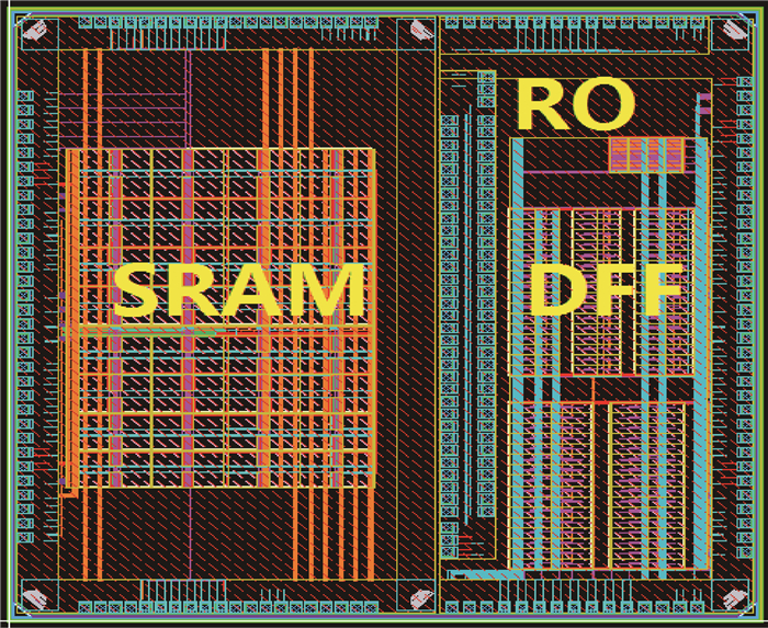
针对功耗和工作频率对22 nm FDSOI背偏和28 nm体硅体偏电路的偏置能力进行对比和分析。以带有4级分频电路的65级环阵(RO)为例进行后仿真,后仿真结果表明,利用背偏技术的22 nm FDSOI环阵的输出频率可在57.8~206 MHz的范围内进行调节,相应的工作电流变化范围为24.4~90.4 μA;而利用体偏技术的28 nm体硅环阵的输出频率调节范围则为92.8~127 MHz,对应的工作电流变化范围为67.8~129 μA。对22 nm FDSOI工艺的环阵进行了实测,实测结果与仿真结果一致。分析认为,在功耗和性能2个方面,22 nm FDSOI电路的背偏调节能力优于28 nm体硅电路的体偏调节能力。
Abstract:In this paper, the body bias circuit in 28 nm bulk and the back bias circuit in 22 nm FDSOI are analyzed and compared from two aspects:power consumption and circuit performance. Taking a 65-stage ring oscillator (RO) with 4-level frequency divider as an example, post simulation was conducted. The simulatior results show that, for 22 nm FDSOI RO using the back bias technology, the output frequency can be adjusted from 57.8 MHz to 206 MHz, with the corresponding operating current varing from 24.4 μA to 90.4 μA, while for 28 nm bulk silicon RO using the body bias technology, the output frequency can be modulated from 92.8 MHz to 127 MHz, with the corresponding operating current varing from 67.8 μA to 129 μA. The 22 nm FDSOI process RO was measured and the measured results are consistent with the simulation results. Therefore, from the view of both power consumption and performance, the adjustment ability of 22 nm FDSOI circuits with back bias is much more efficient than that of 28 nm bulk circuits with body bias.
-
Key words:
- body bias /
- bulk /
- back bias /
- FDSOI /
- ring oscillator (RO)
-
表 1 2种工艺环阵的输出频率对比
Table 1. Comparison of output frequency of RO between two processes
MHz 工艺环阵 最小值 正常值 最大值 28nm体硅CMOS 92.8 120 127 22nm FDSOI 57.8 158 206 表 2 2种工艺环阵的静态电流对比
Table 2. Comparison of standby current of RO between two processes
A 工艺环阵 最小值 正常值 最大值 28 nm体硅CMOS 1.70×10⁻⁸ 2.34×10⁻⁷ 1.26×10⁻⁶ 22 nm FDSOI 1.33×10⁻⁹ 2.99×10⁻⁹ 5.34×10⁻⁹ 表 3 2种工艺环阵的工作电流对比
Table 3. Comparison of operating current of RO between two processes
A 工艺环阵 最小值 正常值 最大值 28nm体硅CMOS 6.78×10⁻⁵ 1.01×10⁻⁴ 1.29×10⁻⁴ 22nm FDSOI 2.44×10⁻⁵ 7.03×10⁻⁵ 9.04×10⁻⁵ 表 4 22 nm FDSOI工艺环阵输出频率仿真与实测对比
Table 4. Comparison of output frequency of 22 nm FDSOI RO between simulation and test
背偏电压/V 输出频率/MHz 仿真值 实测值 (0, 0) 158 154 (+1, 0) 177 175 (+1, -1) 201 193 (+2, 0) 205 195 (+2, -2) 255 239 -
[1] SUN P P, WANG G A, WOODS W, et al.An adaptive body-bias low voltage low power LC VCO[C]//Proceedings of 2010 IEEE International Symposium on Circuits and Systems (ISCAS).Piscataway, IEEE Press, 2010: 1121-1124. [2] HART M J, YOUNG S P, GITLIN D, et al.Structures and methods for selectively applying a well bias to portions of a programmable device: US2003/0053335A1[P].2003-03-27. [3] NABAA G, NAJM F, AZIZI N.FPGA architecture with threshold voltage compensation and reduced leakage: US2008/0180129A1[P].2008-07-31. [4] NEDELCU S, HAUER J, KLEIN L, et al.Dynamic body bias for 22 nm FD-SOI Technology[C]//Proceedings of Analog 2016 IET/GMM-Symposium.Berlin: VDE-Verlag, 2016: 44-48. [5] DE STREEL G, BOL D.Impact of back gate biasing schemes on energy and robustness of ULV logic in 28 nm UTBB FDSOI technology[C]//IEEE International Symposium on Low Power Electronics and Design (ISLPED).Piscataway, NJ: IEEE Press, 2013: 255-260. [6] BERNARD S, BELLEVILLE M, VALENTIAN A, et al.Experimental analysis of flip-flops minimum operating voltage in 28 nm FDSOI and the impact of back bias and temperature[C]//2014 24th International Workshop on Power and Timing Modeling, Optimization and Simulation (PATMOS).Piscataway, NJ: IEEE Press, 2014, 5596: 1-7. [7] CHANG W T, LIN S W, SHIH C T, et al.Back bias modulation of UTBB FDSOI, bulk FinFET, and SOI FinFET[C]//2016 IEEE International Nanoelectronics Conference (INEC).Piscataway, NJ: IEEE Press, 2016: 1-2. [8] SKOTNICHI T.Competitive SOC with UTBB SOI[C]//2011 IEEE International SOI Conference.Piscataway, NJ: IEEE Press, 2011: 1-61. [9] CHRIRAT S, BEIGNE E, BERTHIER F, et al.Ultra low energy FDSOI asynchronous reconfiguration network for an IoT wireless sensor network node[C]//IEEE S3S Microelectronics Technology Unified Conference.Piscataway, NJ: IEEE Press, 2016: 1-3. [10] RASHED M.22FDX FDSOI application towards IOT for smart devices[C]//2017 30th International Conference on VLSI Design and 2017 16th International Conference on Embedded Systems (VLSID).Piscataway, NJ: IEEE Press, 2017. [11] CHEN L, LOMBARDI F, HAN J.FDSOI SRAM cell for low power design at 22 nm technology node[C]//IEEE International Midwest Symposium on Circuits & Systems, College Station. Piscataway, NJ: IEEE Press, 2014: 527-530. [12] SAKURAI T, MATTSUZAWA A, DOUSEKI T.Fully-depleted SOI CMOS circuits and technology for ultra-low power applications[M].Berlin:Springer, 2006:108-113. [13] RABARY J M, ANANTHA C, BORIVOJE N.数字集成电路——电路、系统与设计[M].北京:电子工业出版社, 2012:140-146.RABARY J M, ANANTHA C, BORIVOJE N.Digital integrated circuit-Circuits, systems and designs[M].Beijing:Publishing House of Electronics Industry, 2012:140-146(in Chinese). [14] 黄如, 张国艳, 李映雪, 等.SOI CMOS技术及其应用[M].北京:科学出版社, 2005:168-172.HUANG R, ZHANG G Y, LI Y X, et al.SOI CMOS technology and its application[M].Beijing:Science Press, 2005:168-172(in Chinese). [15] GAO C, ZHAO X, ZHAO K, et al.DSOI-A novel structure enabling adjust circuit dynamically[J].Journal of Semiconductor, 2016, 37(6):065003. doi: 10.1088/1674-4926/37/6/065003 -


 下载:
下载:
