


基于自适应积分电容的高动态像素结构研究
doi: 10.13700/j.bh.1001-5965.2023.0349
Structure research on the high dynamic pixel based on adaptive integral capacitance
 下载:
下载:

 点击查看大图
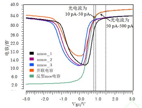
图(1)
计量
- 文章访问数: 78
- HTML全文浏览量: 32
- PDF下载量: 0
- 被引次数: 0
